22-February-2024
The
focus ring is an important component placed outside the wafer and in
direct contact with the wafer. By applying a voltage to the ring to
focus the plasma passing through the ring, the plasma is focused on the
wafer to improve the uniformity of the process.
CVD
silicon carbide parts in etching equipment include focusing rings, gas
shower heads, trays, edge rings, etc. Due to the low reactivity and
conductivity of CVD silicon carbide to chlorine- and fluorine-containing
etching gases, it becomes a plasma Ideal material for components such
as focus rings in etching equipment.
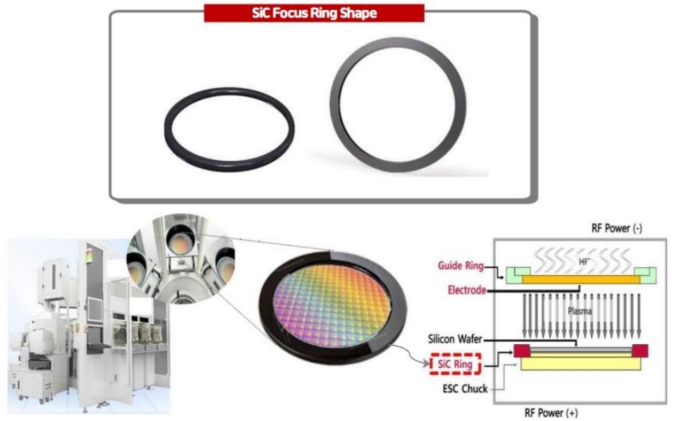
Figure 1: Application of silicon carbide focusing ring in etching machine
Silicon
carbide is an ideal material for the focus ring. Since the focus ring
will directly contact the plasma in the vacuum reaction chamber, it is
necessary to use materials that are resistant to plasma corrosion.
Traditional focus rings are made of silicon or quartz. Conductive
silicon is a commonly used focus ring material. Its conductivity is
almost close to that of silicon wafers. However, its disadvantage is
that it has poor etching resistance in fluorine-containing plasma. The
material of etching machine parts Serious corrosion will occur after
being used for a period of time, seriously reducing its production
efficiency.
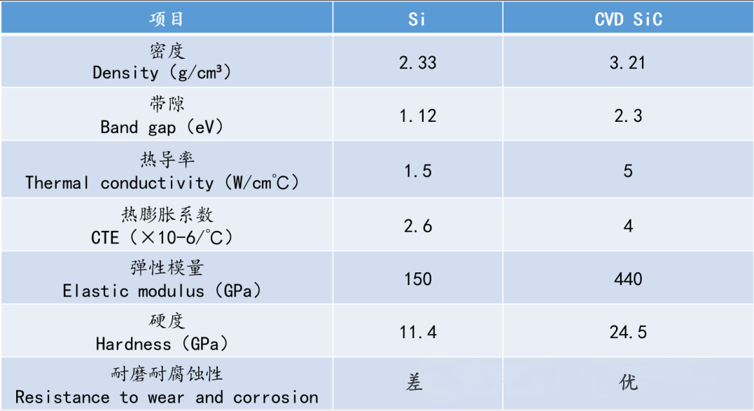
Figure 2 Comparison between Si-based focusing ring and CVD SiC focusing ring
SiC focusing rings are better than traditional Si in terms of mechanical properties, chemical properties, thermal conductivity, high temperature resistance, and ion etching resistance:
(1) High density reduces etching amount;
(2) Higher band gap and excellent insulation;
(3) High thermal conductivity, low expansion coefficient, and thermal shock resistance;
(4) High elasticity and good resistance to mechanical impact;
(5) High hardness, wear resistance and corrosion resistance.
Silicon
carbide has similar conductivity to silicon and good resistance to ion
etching. As the miniaturization of integrated circuits advances, the
demand and importance of etching processes for integrated circuit
manufacturing continue to increase. The power and energy of plasma used
for etching continue to increase, especially those required in
capacitively coupled (CCP) plasma etching equipment. The plasma energy
is higher, so the focus ring made of silicon carbide material is
increasingly used.
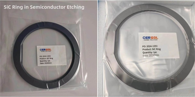
Figure 3 Solid Silicon Carbide Focusing Ring
In the field of silicon carbide components for semiconductor equipment, companies in the industry generally use the chemical vapor deposition (CVD) method for production. Usually, the focus ring is made by depositing the silicon carbide generated by chemical reaction into a certain shape through vapor deposition method, and then machining the silicon carbide in a certain shape according to the specific use conditions to generate the focus ring. In this process, the ratio of raw materials involved in vapor deposition is fixed after many experiments, so the properties of the silicon carbide focusing ring produced, such as resistivity and other parameters, are also fixed. However, for plasma etching equipment, the fixed resistivity is not always applicable to different etching equipment. When a focus ring with a lower resistivity or a focus ring with a higher resistivity is required, the gas phase involved needs to be changed. The ratio of deposited raw materials requires multiple experiments to re-determine the ratio of raw materials, which takes a long time and costs a lot.