Technical Article
Y2O3 Plasma-Resistant Coatings for Semiconductor Etching Equipment
Y2O3, or yttria, is used as a plasma-resistant ceramic coating and bulk material for semiconductor etch-chamber components. In fluorine-containing plasma, its surface can form low-volatility yttrium fluoride and oxyfluoride species that slow further attack. Actual coating life and particle performance depend on deposition method, porosity, purity, roughness, adhesion, thickness, substrate, chamber position, and the specific plasma recipe.
Key Takeaways
- Y2O3 is valuable because fluorinated yttrium surface products are generally less volatile than aluminum fluoride, helping limit erosion and contamination in aggressive plasma environments.
- A dense, well-adhered coating can protect an aluminum or ceramic component without the cost and manufacturing constraints of a fully dense bulk-yttria part.
- APS, aerosol deposition, PVD, CVD, and ALD create very different thicknesses, microstructures, surface finishes, and coverage on complex geometry.
- Y2O3 is not automatically the best option. YF3 or YOF can perform better in some fluorine-rich conditions, while YAG may offer a useful corrosion-mechanical balance.
- An RFQ should define the plasma chemistry, RF power, pressure, duty cycle, component location, substrate, geometry, allowable particles, cleaning method, and acceptance tests.
Contents
- Why plasma-facing chamber parts need protection
- Why Y2O3 resists fluorine plasma
- Y2O3 coating or bulk yttria ceramic?
- How Y2O3 coatings are deposited
- Y2O3 vs Al2O3, YF3, YOF, and YAG
- Where Y2O3 is used in semiconductor equipment
- What to specify when selecting a coating
- Failure modes and limitations
- RFQ checklist
- Frequently asked questions
Why Plasma-Facing Chamber Parts Need Protection
Dry etching uses reactive species and energetic ion bombardment to remove material with tight profile control. Fluorine-containing chemistries such as CF4, CHF3, C4F6, SF6, and NF3 are common across dielectric etch, silicon etch, and chamber cleaning. For a broader process explanation, see why semiconductor dry etching requires fluorine plasma.
The same plasma can attack chamber liners, shields, windows, focus rings, showerheads, and electrostatic-chuck surroundings. Chemical reaction and physical sputtering change the exposed surface. Consequences include:
- eroded material can become particles or metallic contamination;
- roughening and local damage can make particle release less predictable;
- deposits and reaction layers can flake during cycling or cleaning;
- changes in wall condition can alter plasma impedance and process stability;
- shorter maintenance intervals reduce equipment availability.
The objective is not merely the lowest coupon etch rate. A useful chamber material must also control particles, survive thermal and plasma cycles, tolerate cleaning, preserve its functional geometry, and remain manufacturable.
Why Y2O3 Resists Fluorine Plasma
Yttrium oxide is a refractory rare-earth oxide with a melting point commonly reported near 2,430 °C. More important for plasma equipment is its surface chemistry. When Y2O3 is exposed to fluorine-containing plasma, oxygen near the surface can be replaced by fluorine, producing a thin reaction region containing YF3 and intermediate yttrium oxyfluorides such as YOF.
This fluorinated layer can act as a passivation barrier because yttrium fluoride species are relatively stable and less volatile than the aluminum fluoride products formed on Al2O3. A 2025 study of sputtered Y2O3 films cites sublimation enthalpies of 481 ± 21 kJ/mol for YF3 and 301 ± 4 kJ/mol for AlF3, helping explain why fluorinated yttria surfaces can reduce material loss under relevant conditions. The study also showed that deposition temperature and resulting film structure strongly changed plasma-etch depth, so the chemistry cannot be separated from the coating microstructure. Read the study in Coatings.
Passivation does not mean zero erosion. Ion energy, radical density, gas, pressure, bias, temperature, and exposure time all matter. Pores, splat boundaries, microcracks, and weak interfaces can still expose fresh material or release particles.
The practical conclusion is simple: specify a coating system, not just a chemical formula.
Y2O3 Coating or Bulk Yttria Ceramic?
Coatings and bulk ceramics solve different design problems.
| Option | Main advantages | Main constraints | Typical fit |
|---|---|---|---|
| Y2O3 coating on aluminum | Protects large or complex metal parts; substrate retains structural function; refurbishment may be possible | Coating adhesion, pores, edge coverage, thickness uniformity, thermal-expansion mismatch, and surface preparation must be controlled | Chamber liners, shields, covers, large housings |
| Y2O3 coating on ceramic | Combines substrate properties with a plasma-resistant surface | Interface compatibility and coating damage during handling or cleaning remain important | Windows, rings, dielectric components, specialty fixtures |
| Bulk Y2O3 ceramic | No coating interface; composition extends through the part; can be finished to controlled geometry and surface | High raw-material and sintering cost; brittleness; difficult machining; size and shape constraints | Smaller high-value rings, windows, liners, inserts, or components needing through-thickness chemistry |
Choose bulk material when a coating interface is unacceptable or the component needs yttria chemistry throughout. Choose a coating when the substrate already supplies the required strength, thermal response, geometry, or lower cost.
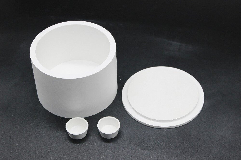
Cersol Y2O3 ceramic is offered for semiconductor chamber rings, linings, coatings, etchers, and ion-implantation equipment. Published product-page values should be treated as grade-specific data and confirmed on the final drawing and test method before design release.
How Y2O3 Coatings Are Deposited
The deposition route determines whether the result is a thick lamellar barrier, a dense impact-consolidated layer, or a thin conformal film.
| Method | Typical engineering character | Strengths | Main watch-outs |
|---|---|---|---|
| Atmospheric plasma spray (APS) | Thick, lamellar coating built from molten or semi-molten powder splats | High deposition rate; practical for large chamber parts; can build substantial thickness | Pores, splat boundaries, microcracks, roughness, unmelted particles, and line-of-sight effects require control |
| Aerosol deposition | Dense ceramic layer formed by high-velocity room-temperature particle impact | Low process temperature; fine microstructure; useful where substrate heating is limited | Residual stress, achievable thickness, equipment scale, and complex-feature coverage must be qualified |
| PVD / reactive sputtering | Thin, comparatively dense line-of-sight film | Smooth finish; controlled composition; useful for precision surfaces | Lower thickness and slower build than thermal spray; shadowing on complex geometry; process cost |
| CVD | Dense film produced from gaseous precursors | Good purity and film continuity; potential for more uniform coverage than direct line-of-sight spray | High process temperature or precursor constraints; reactor compatibility; cost and size limits |
| ALD | Very thin, highly conformal film deposited cycle by cycle | Excellent coverage of high-aspect-ratio or complex surfaces; precise thickness control | Low deposition rate; thin-film pinholes or defects matter; thick protective builds can be uneconomic |
APS remains attractive for large-area chamber hardware, but "plasma-sprayed Y2O3" does not define one performance level. Powder, spray energy, surface preparation, cooling, grinding, and cleaning all affect the result.
Thin films can be smoother and denser, but may lack sacrificial thickness. Hybrid designs combine a structural or anodized base with a dense Y2O3-containing film. A 2025 anodization-and-ALD study reported YF3/YOF passivation and improved hardness and etch resistance in its test system. Apply those results only after recipe-specific qualification. See the Ceramics International study.
Y2O3 vs Al2O3, YF3, YOF, and YAG
Material selection should reflect the plasma chemistry and the dominant failure mode, not a universal ranking.
| Material | Why engineers consider it | Where it may be favored | Qualification concern |
|---|---|---|---|
| Al2O3 | Established supply chain, mechanical robustness, broad component availability, lower cost | Less aggressive zones, structural ceramics, anodized aluminum systems, cost-sensitive hardware | Fluorine plasma can form more volatile AlF3; erosion and aluminum-containing particles may be unacceptable in critical zones |
| Y2O3 | Stable rare-earth fluoride/oxyfluoride surface products; established semiconductor use; available as coating and bulk ceramic | Fluorine-plasma-facing liners, rings, windows, shields, and protected metal hardware | Performance is sensitive to porosity, cracks, surface finish, adhesion, and recipe conditions |
| YF3 | Surface starts in a fluorinated state; can reduce oxygen-related chemistry and show strong fluorine-plasma resistance | Fluorine-rich environments where erosion and particle data justify it | Moisture handling, deposition behavior, mechanical integrity, thermal cycling, and supply route require validation |
| YOF | Intermediate oxyfluoride composition can balance oxide processing with fluorinated surface chemistry | Applications seeking lower particle generation or more stable surface conversion | Composition control, phase stability, deposition repeatability, and limited standardized data |
| YAG (Y3Al5O12) | Dense garnet ceramic can combine yttrium chemistry with useful mechanical properties | Bulk parts or dense coatings where mechanical durability and corrosion resistance must be balanced | Contains aluminum; performance depends on phase purity and whether Al-containing reaction products matter |
In a high-density CF4/O2 plasma study, APS YF3 produced fewer contamination particles than APS Y2O3 under the tested conditions. The Y2O3 coating also contained cavities and cracks that influenced erosion. This does not prove that YF3 always wins; composition and as-sprayed microstructure must be evaluated together. Review the open-access comparison.
YAG is another useful alternative rather than a simple compromise. A 2024 study reported that a dense yttrium-aluminosilicate coating containing 77.64% YAG reduced normalized mass loss from 0.0148%/cm2 for uncoated alumina to 0.0047%/cm2 after one hour in a C4F6/Ar/O2 plasma test. The approximately threefold improvement belongs to that coating and test condition, but it supports YAG-containing systems as valid candidates. Read the Materials study.
Where Y2O3 Is Used in Semiconductor Equipment
The component location changes the design priority.
| Component | Why Y2O3 may be used | What to verify |
|---|---|---|
| Chamber liners and shields | Reduce wall erosion and metal contamination over large exposed areas | Coating uniformity, edge treatment, thermal cycling, cleanability, repair strategy |
| Focus rings and edge rings | Protect a high-field, high-ion-flux region near the wafer edge | Dimensional tolerance, surface finish, local erosion profile, particle behavior, bulk vs coating choice |
| Dielectric or RF windows | Combine plasma resistance with an electrically insulating function | Dielectric properties at frequency, thickness uniformity, porosity, thermal gradient, arcing history |
| Showerheads and gas-distribution parts | Protect plasma-facing surfaces and gas openings | Hole coverage, blocked or rounded features, coating thickness inside openings, flake risk |
| Electrostatic-chuck surroundings | Reduce contamination near the wafer and protect adjacent structures | Electrical isolation, flatness, thermal expansion, backside compatibility, particle limits |
| Covers, baffles, and confinement hardware | Extend maintenance intervals in exposed but geometry-sensitive areas | Line-of-sight coverage, masking, fastener interfaces, assembly damage |
For RF and microwave plasma hardware, coating chemistry must also be considered alongside field distribution and dielectric loss. See how RF and microwave plasma interact with ceramic chamber components.
What to Specify When Selecting a Coating
1. Plasma and process conditions
Provide the full gas family and approximate ratios where confidentiality permits, including cleaning gases. Add RF source and bias power, pressure range, substrate or wall temperature, duty cycle, and expected exposure hours. A CF4/O2 coupon result may not predict behavior in NF3 cleaning, chlorine plasma, mixed halogen chemistry, or a different ion-energy regime.
2. Purity and contamination limits
State the required Y2O3 purity and identify restricted elements. Bulk chemical purity alone is not enough; powder handling, spray hardware, grinding media, masking, cleaning, packaging, and substrate exposure can add contaminants. Ask how the supplier verifies both feedstock and finished coating.
3. Density, porosity, and microstructure
Define the measurement method and acceptance region. Average porosity can hide connected pores, local voids, microcracks, or weak splat boundaries. Request cross-sectional images at representative locations and near edges, holes, and transitions.
4. Thickness and uniformity
Specify nominal thickness, tolerance, masked areas, edge transition, and measurement points. More thickness is not always better: it can increase residual stress, change dimensions, make thermal mismatch more severe, and require additional finishing.
5. Surface roughness and finishing
Surface roughness influences effective plasma-exposed area, deposit adhesion, cleaning response, and particle release. Define Ra or another relevant parameter after final grinding, polishing, or conditioning, not only in the as-deposited state.
6. Adhesion and thermal compatibility
The substrate material, pretreatment, interface design, coating thickness, and operating temperature determine stress. Specify an adhesion test where appropriate, but also request thermal-cycle and process-simulation evidence because a room-temperature pull value does not reproduce chamber service.
7. Geometry and functional interfaces
Send a controlled drawing. Mark plasma-facing surfaces, sealing faces, O-ring grooves, threads, holes, electrical interfaces, datum surfaces, no-coat zones, edge radii, and post-coating dimensions. Complex geometry may favor a conformal thin-film method or a hybrid design rather than APS alone.
8. Acceptance evidence
Agree on incoming inspection before production: thickness map, roughness, porosity, phase or composition data, adhesion evidence, cleanliness, visual criteria, packaging, and coupon traceability. For critical parts, define a chamber or plasma-coupon qualification that measures erosion and particles under a representative recipe.
Failure Modes and Limitations
Y2O3 solves a chemical-corrosion problem, but it does not remove the mechanical and manufacturing limits of ceramic systems.
- Pores and connected pathways: Plasma can attack weak regions or reach the underlying substrate through defects.
- Cracking and delamination: Residual stress, thermal-expansion mismatch, poor surface preparation, excessive thickness, or thermal cycling can damage the interface.
- Particle shedding: Rough peaks, weak splats, reaction products, redeposited films, and cleaning damage can all release particles.
- Edge erosion: Sharp transitions, holes, and line-of-sight shadow regions may receive nonuniform coverage and concentrated plasma exposure.
- Process drift: A coating can change as it conditions, fluoridates, accumulates deposits, or is cleaned. Initial and steady-state behavior may differ.
- Bulk-ceramic brittleness: Fully dense Y2O3 avoids delamination but remains brittle and can be costly to sinter and machine in large, tight-tolerance shapes.
- Data-transfer risk: Supplier data may use different plasma density, ion energy, gas mixture, coupon geometry, exposure time, and endpoint. Compare test conditions before comparing numbers.
The strongest evidence is not a "zero erosion" claim. It is a traceable link between coating process, finished microstructure, representative plasma testing, particles, and production acceptance criteria.
RFQ Checklist
Send the following information when requesting a Y2O3 plasma-resistant coating or bulk yttria component:
- part name, drawing revision, quantity, and replacement or new-design status;
- substrate material and temper, or requested bulk-ceramic grade;
- plasma gases, cleaning gases, approximate ratios, pressure, source power, and bias power;
- continuous and peak temperatures, thermal-cycle range, and exposure hours;
- plasma-facing surfaces, no-coat zones, holes, grooves, threads, seals, and critical datums;
- target thickness and tolerance, final dimensions, flatness, and edge requirements;
- required purity and restricted-element limits;
- surface roughness target and whether it applies before or after plasma conditioning;
- porosity, adhesion, composition, cleanliness, and inspection methods;
- particle limit, erosion target, or incumbent benchmark with its test method;
- cleaning, refurbishment, packaging, and handling requirements;
- qualification quantity and acceptance plan before production release.
This information allows a supplier to determine whether APS Y2O3, a denser deposition route, a YF3/YOF alternative, a multilayer system, or a bulk ceramic is the better engineering answer.
Selecting a Y2O3 plasma-resistant coating should therefore be treated as a matched-system decision: plasma chemistry, coating microstructure, interface design, component geometry, and acceptance evidence must work together. When those variables are defined before sourcing, engineers can compare Y2O3 fairly with Al2O3, YF3, YOF, and YAG instead of selecting a chamber material by name alone.
Frequently Asked Questions
Need custom Y2O3 ceramic component or plasma-resistant coating support?
Contact Our TeamEngineering References
- Lin et al., "Comparison of Erosion Behavior and Particle Contamination in Mass-Production CF4/O2 Plasma Chambers Using Y2O3 and YF3 Protective Coatings," *Nanomaterials*, 2017. https://pmc.ncbi.nlm.nih.gov/articles/PMC5535249/
- "Preparation and Characterization of Y2O3 Films for Semiconductor Equipment," *Coatings*, 2025. https://www.mdpi.com/2079-6412/15/12/1397
- "Plasma-resistant and mechanical properties of Al2O3-Y2O3 multilayer coatings fabricated by anodization and atomic layer deposition," *Ceramics International*, 2025. https://www.sciencedirect.com/science/article/pii/S0272884225024290
- Lee et al., "Plasma-Resistant Yttrium-Aluminosilicate Glass-Ceramic Coating on Alumina," *Materials*, 2024. https://pmc.ncbi.nlm.nih.gov/articles/PMC11432973/