17-April-2024
With the rapid development of information technology and the growing demand for high-efficiency electronic devices, the third generation of semiconductor materials represented by silicon carbide (SiC), with its bandgap width, dielectric constant, thermal conductivity and highest operating Advantages in aspects such as temperature are gradually emerging. However, as a typical hard and brittle material, silicon carbide is much harder than traditional silicon materials, with a Mohs hardness of up to 9.2, second only to the world’s hardest diamond, which makes its wafer manufacturing process certain challenges.
The current manufacturing process of silicon carbide wafers is divided into: cutting - grinding - polishing - cleaning. At each processing stage, there are certain requirements for surface damage and roughness. Among them, cutting is the first step in processing silicon carbide single crystal wafers. The processing quality of the primary process will have a great impact on the subsequent grinding and polishing processing levels, thereby affecting the performance of the chip. In current industrial production, silicon carbide wafers are generally cut using multi-line cutting methods. With the continuous advancement of technology, new cutting technologies such as water-guided laser cutting and invisible cutting have also emerged.
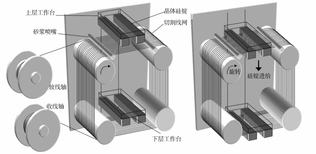
Multi-wire cutting technology
Multi-wire cutting technology is the current mainstream wafer cutting technology. Compared with the previous saw blade cutting method, it overcomes the shortcoming of only cutting one wafer at a time. At present, according to the cutting materials, there are two main methods: free abrasive wire saw cutting (mortar wire cutting) and diamond wire saw cutting.
Multi-line cutting diagram
01 Free abrasive wire saw cutting
The cutting process of free abrasive wire saw is a complex process of interaction between the cutting wire, the abrasive in the cutting fluid and the workpiece. The cutting mechanism is to use the rapid movement of the wire saw to bring the abrasive particles in the cutting fluid into the saw kerf. Driven by the pressure and speed, the free abrasive particles continuously roll in the saw kerf, thereby cutting the material. When using this technology to cut silicon carbide ingots, the abrasive grains that act as cutting blades have a great impact on the cutting effect. Due to the extremely high hardness of silicon carbide, the cutting fluid needs to use diamond powder as abrasive grains to achieve a more efficient result. For the purpose of cutting, mortar, as a carrier of abrasive particles, plays a role in stably dispersing and driving movement of the abrasive particles suspended in it, so it has certain requirements for its viscosity and fluidity.
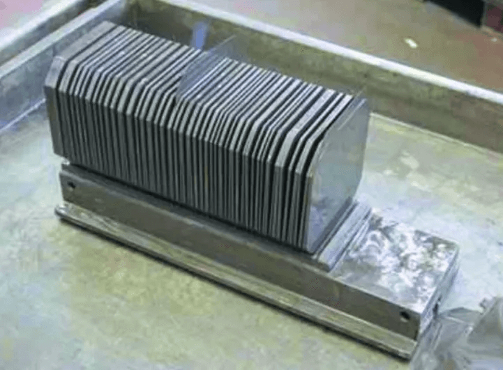
Wafer after free abrasive multi-line cutting
Among them, the cutting lines of free abrasive multi-wire cutting mostly use Cu-plated stainless steel wires (Ф150~300 μm), and the total length of a single wire can reach 600~800 km. Mortar is mainly made of 10-15 μm silicon carbide or diamond and mineral oil or water mixed in a certain proportion.
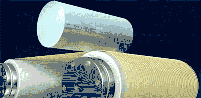
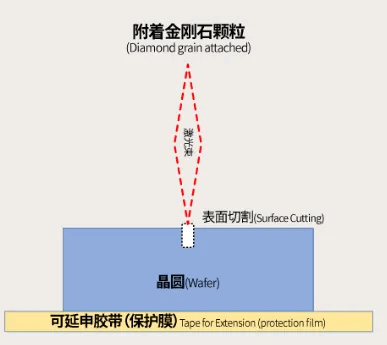
02 Consolidated diamond wire saw cutting
Due to the shortcomings of low cutting speed and low abrasive grain utilization, free abrasive wire saws are gradually replaced by diamond wire saws. Diamond wire saw cutting uses high-hardness, high-wear-resistant diamond abrasive grains to be fixed on the cutting line through methods such as electroplating, resin bonding, brazing or mechanical inlaying. Through the high-speed reciprocating movement of the diamond wire, the abrasive grains are directly connected to the workpiece. Relative grinding motion is formed between them, thereby completing the cutting of the SiC ingot.
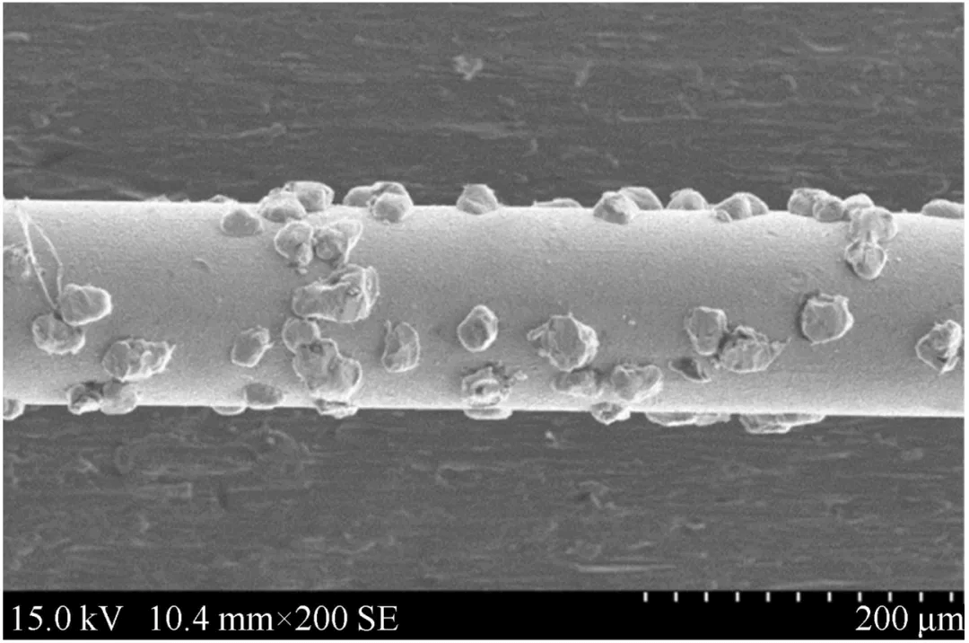
Fixed abrasive diamond wire
Compared with the "three-body processing" of free abrasive wire saw cutting, fixed diamond wire saw cutting belongs to "two-body processing". Its processing efficiency is several times more than that of free abrasive wire saw cutting, and it has narrow cutting slits and less environmental pollution. Etc. However, when cutting hard and brittle materials such as SiC using this method, there are still shortcomings such as deep damage to the wafer surface and rapid wire saw wear. When the diamond wire is severely worn during the wire saw cutting process, it will greatly affect the performance of the wire saw. lifetime and wafer warpage. Therefore, the fixed diamond abrasive wire saw technology is not suitable for producing ultra-thin and large-sized SiC single crystal wafers.
New wafer laser cutting technology
In recent years, with the continuous development of laser cutting technology, this non-contact cutting technology has been increasingly used in the production and processing of semiconductor materials. For example, the successful application of laser stealth cutting technology for sapphire and silicon wafers has provided Silicon carbide (SiC) wafer cutting technology provides new solutions and has derived a variety of processing methods for laser cutting silicon carbide (SiC) wafers.
01 Invisible laser cutting technology
Traditional laser cutting is a full cutting processing method that concentrates laser energy on the surface of the material in a very short period of time to sublimate and evaporate the solid. It belongs to laser ablation processing technology. The principle of laser stealth cutting is to use pulsed laser of a specific wavelength to focus inside the material through the surface of the material, generating a higher energy density in the focus area, forming multi-photon absorption, and forming a modified layer at the required depth within the material. At the location of the modified layer, due to the destruction of the molecular bonds of the material, when pressure is applied perpendicular to the strip-shaped modified layer, the ingot will be divided into thin slices along the crack trajectory.
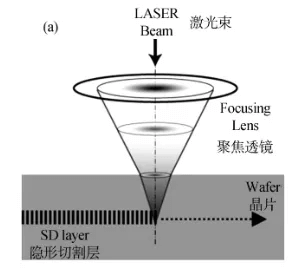
Comparison of the principles of traditional laser and laser invisible cutting technology
Since laser stealth cutting technology performs non-contact modification inside the ingot, it can suppress the generation of processing chips, which not only prevents the wafer from being contaminated, but also avoids damage to the wafer caused by chips. At the same time, stealth cutting is considered to be zero line width cutting. , compared with traditional laser cutting technology, it effectively solves the problems of cutting damage and large micro-cracks, and provides a faster, more stable and more reliable solution for large-scale preparation of thin silicon carbide wafers. However, as a new type of laser cutting technology, laser hidden cutting technology still faces a series of problems that need to be solved during the application process, such as wafer surface warpage and laser energy density control problems, which will cause the laser focus to fail to accurately fall on the wafer. The specific thin layer hinders the further improvement of cutting accuracy and chip yield; in order to avoid that longer laser pulse duration will produce a larger thermal effect, leading to wafer breakage and poor peeling offset, it is necessary to use higher-cost ultra-short laser pulses. Pulse laser to achieve hidden cutting.
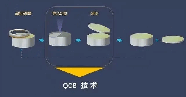
Han’s Semiconductor combines laser hidden cutting technology and ultrafast laser to develop new laser dicing (QCB technology) technology
02 Water guide laser cutting technology
Water-guided laser cutting technology, also known as laser microjet technology, its principle is to focus the laser beam on a very small nozzle when the laser passes through a pressure-modulated water cavity, and spray an extremely fine high-pressure water column from the nozzle , due to the total reflection phenomenon occurring at the interface between water and air, the laser will be constrained in the fine water jet, and conducted and focused through the water jet, thereby guiding the laser to cut on the surface of the processed material through the high-pressure water jet.
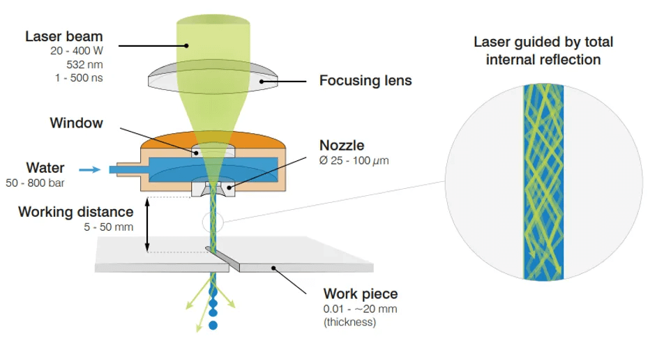
Water guide laser cutting principle
Due to the existence of micro-jet, water-conducted laser technology can not only cool the cutting area and reduce the degree of thermal deformation and thermal damage of the material, but also take away processing debris, reduce wafer contamination, and achieve extremely high cutting quality. Usually end face roughness is common It can be controlled within the range of Ra<1μm. However, due to the difficulty of coupling micro-water guide laser cutting technology, in order to improve the laser utilization efficiency, it is not only necessary to ensure that the laser beam enters the nozzle mouth to the maximum extent, but also to achieve total reflection as much as possible, which requires high process accuracy.
Large-size single crystal SiC substrates are the mainstream development trend in the future. At present, domestic mainstream SiC companies have basically achieved full growth of 6 inches and are developing rapidly in the direction of 8 inches. At present, the most widely used method for slicing silicon carbide ingots in industry is solidified diamond multi-wire cutting. When cutting large-size wafers, solidified diamond wires are prone to wear and have a certain impact on the cutting quality of the wafers. In recent years, various new laser processing technologies such as laser stealth cutting and water-guided laser cutting have provided reliable solutions for cutting large-size silicon carbide wafers with the advantages of high cutting quality, low cutting damage, and high efficiency.
Product page:https://www.ceramic-solutions.com/Boron-Nitride.html
Contact page:https://www.ceramic-solutions.com/Contact.html