13-January-2026
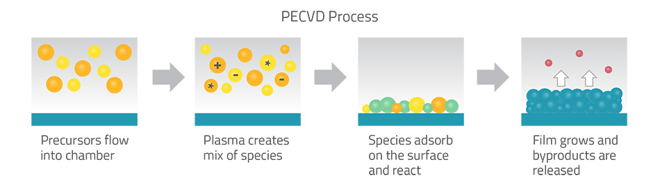 Traditional thin-film processes like PECVD flood the reaction chamber with gases in one shot. For example, PECVD uses a plasma to energize reactant gases that form a “soup” of reactive fragments coating the wafer. This fast, high-temperature process can deposit films quickly, but it’s hard to control thickness at the atomic level. ALD takes a different approach: it splits the deposition into two alternating, self‑limiting steps. First one precursor gas is introduced and it adsorbs onto the surface until no more sites remain (self-limiting). Then a second reactant is added, which reacts with that first layer to form one atomic layer of the target material. Each step stops automatically when the surface is fully covered. By repeating these two half-reactions over and over, ALD builds up an ultra-thin film, one atomic layer at a time.
ALD follows a precise cycle of four steps. A typical sequence is:
1. Precursor A dosing: Introduce precursor A into the chamber so it adsorbs onto all exposed surfaces until it saturates.
2. Purge: Flush the chamber with an inert gas to remove any excess precursor A and reaction by-products.
3. Precursor B dosing: Introduce precursor B, which reacts with the adsorbed layer of A to form the desired thin film layer.
4. Purge: Again, use inert gas to clear out unused precursor B and by-products.
Each complete cycle deposits roughly one atomic layer of material. By repeating these steps dozens or hundreds of times, engineers can precisely “dial in” the film thickness in nanometers or less.
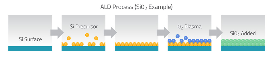
As the figure above (from Lam Research) illustrates for silicon dioxide, one ALD cycle might use a silicon-containing precursor followed by an oxygen step. First the silicon precursor coats the wafer surface (steps 1–3), then an oxygen source converts it to SiO₂ (steps 4–5). Repeating this cycle deposits a uniform oxide film one ultra-thin layer at a time.
ALD’s layer-by-layer chemistry gives it some special advantages:
- Atomic-scale precision: Each ALD cycle deposits a known, tiny amount of material (often ~1 Å per cycle), so film thickness can be controlled to within a few atoms. Engineers simply count cycles to “tune” thickness very precisely.
- Exceptional uniformity: ALD films are extremely uniform across the wafer. Lam Research notes that ALD can yield “identical film thicknesses” on the tops, sides, and bottoms of 3D features. In practice this means an ALD coating in a deep trench is as thick at the bottom as at the top edge.
- Excellent conformality: ALD naturally coats every surface evenly, even inside very narrow holes or around complex 3D shapes. This high conformality is critical for coating high-aspect structures (deep trenches, vias, or nanostructured surfaces) without gaps or pinholes.
- Smooth, pinhole-free films: The self-limiting reactions produce very smooth and dense films. Surfaces created by ALD are “atomically smooth” with no pinholes. This high film quality is crucial in semiconductors and optics where any defect can cause failures.
- Low-temperature processing: Many ALD reactions occur at relatively low temperatures (often 50–500 °C). This is gentle on heat-sensitive substrates (like certain polymers or pre-fabricated devices) and enables coating of materials that can’t tolerate high heat.
- Reproducibility: Because each half-reaction self-terminates, ALD processes are highly repeatable. A well-tuned ALD recipe will deposit the same film on every wafer, aiding manufacturing yield.
These features are hard to achieve with other methods. For example, PECVD and sputtering can coat faster but usually lack ALD’s atomic control and coverage. In fact, ALD is often called the method of choice when “atomic-level control and perfect coverage” are needed on complex structures.
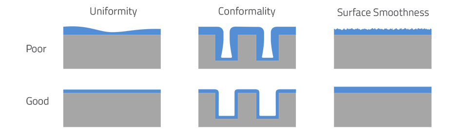
The figure above contrasts poor vs. good film coverage: on the left, uneven deposition and roughness occur with conventional processes, while on the right the ALD coating is flat and uniform (smooth line) with even thickness around edges. ALD achieves this “good” result naturally, because each step stops exactly when the surface is filled.
Thanks to these strengths, ALD has found use in many high-tech fields:
- Semiconductors & electronics: ALD is widely used in chip manufacturing for transistors and memory devices. It deposits ultra-thin gate dielectrics, spacers and barrier layers with tight tolerances. For example, ALD is used to form the conformal thin liners in 3D NAND flash holes and the gate spacers in FinFET transistors. In each case, ALD ensures uniform coverage in very narrow features where traditional CVD or sputtering would fail.
- Batteries and energy storage: Uniform, conformal coatings can greatly improve battery electrodes and interfaces. ALD can apply protective or functional layers on lithium-ion battery materials and solid electrolytes. As noted by Veeco, thin ALD coatings on electrodes support smooth ion flow, enabling batteries to store more energy and last longer. Such layers can also prevent unwanted reactions, boosting safety and cycle life.
- Optics and photonics: ALD can make high-quality anti-reflection or protective coatings on optical components, even on curved or 3D shapes. Unlike line-of-sight methods (e.g. sputtering), ALD uniformly covers lenses, domes or waveguides. For instance, Beneq reports that ALD deposited broadband AR stacks on dome-shaped optics with ultra-low reflectance. This yields superb optical performance on geometries that would be impossible with conventional techniques.
- MEMS and sensors: Micro-electromechanical systems (MEMS) and sensors often have tiny moving parts or cavities that need thin films (insulators, passivation layers, etc.). ALD’s conformality makes it ideal for coating these microstructures uniformly, improving device reliability and performance.
- Other fields: ALD is also used in advanced photovoltaics (thin buffer layers), flexible electronics, catalysis, and even medical implants (biocompatible coatings). In general, any application requiring a pinhole-free nano-scale film on a complex surface can benefit from ALD.
Advantages: ALD’s biggest draw is its combination of precision and uniformity. It can coat literally every nook and cranny of a 3D structure with atomic-scale control. This yields ultra-thin layers with minimal defects, which is essential for next-generation electronics, energy devices and optics. ALD films also tend to be very uniform and reproducible across large substrates.
Limitations: The main drawback of ALD is throughput. Because each cycle deposits only a tiny amount, building up a thick film (tens of nanometers) can take many minutes or hours. In other words, ALD is much slower than CVD or sputtering for a given thickness. The specialized precursors used in ALD can also be costly or difficult to handle, and the equipment is more complex. In practice, engineers weigh these trade-offs: if utmost uniformity and atomic control are required, ALD is worth the extra time and cost; if a quick, thick coating is acceptable, other methods may be chosen.
In comparison, PECVD or PVD can deposit films faster and at lower cost, but they cannot achieve ALD’s level of control in deep structures. Castmold’s comparison sums it up: ALD “is the method of choice when you need atomic-level control and perfect coverage in complex 3D structures”.
Atomic Layer Deposition (ALD) is a thin-film technique that literally builds materials one atomic layer at a time. By alternating self-limiting chemical steps, ALD achieves atomic-scale thickness control and unmatched uniformity. It enables high-quality, conformal coatings on even the most complex surfaces, which is why it’s used in advanced chips, batteries, optics and more. The trade-off is its slower deposition rate and higher process cost. But for the tiniest, most precise devices of the future, ALD’s ability to lay down atoms exactly where they belong makes it an indispensable tool in modern material science.