16-January-2026
Vapor Phase Epitaxy (VPE) is a cornerstone technology in the semiconductor industry, acting as a high-tech "builder" that constructs materials atom by atom. The term "epitaxy" refers to the neat arrangement of atoms on a substrate, and in the VPE process, this construction happens entirely through the gas phase. Unlike traditional methods that melt materials down, VPE allows engineers to grow ultra-thin, high-purity crystal layers that inherit the perfect structure of the blueprint beneath them. This "atomic mimicry" is what makes VPE indispensable for creating the complex electronic and optical components found in everything from smartphones to electric vehicles.
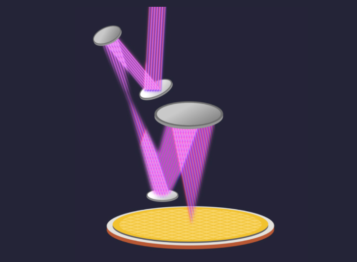
The principle of VPE begins with the delivery of chemical precursors in gaseous form. In a VPE reactor, these gases carry the necessary elements—such as Gallium, Arsenic, or Nitrogen—into a highly controlled chamber. In some VPE variants, liquid metals are reacted with gases to create vapors, while in others, specialized metal-organic molecules are used. These VPE precursors are transported by a carrier gas, usually ultra-pure hydrogen, toward a heated wafer. This gas-phase delivery is the secret to VPE’s precision, allowing for the creation of layers that are sometimes only a few atoms thick.
A fascinating part of the VPE process is the "boundary layer" phenomenon. As the precursor gases flow through the VPE reactor, they encounter a thin, stagnant layer of gas just above the hot wafer. To grow a crystal, the precursor molecules must diffuse through this VPE boundary layer to reach the surface. By adjusting the pressure within the VPE reactor, engineers can control the thickness of this layer. Thinner layers allow for faster and more uniform growth, which is why many modern VPE systems operate at low pressures to ensure the highest possible material quality.
Once the molecules reach the hot surface, a process called pyrolysis occurs. The intense heat of the VPE reactor breaks the chemical bonds of the precursors, releasing the "building block" atoms. These atoms don't just stick randomly; they move across the surface until they find the perfect spot in the crystal lattice. This surface diffusion ensures that the new VPE layer is a perfect continuation of the substrate's crystal structure. Meanwhile, the leftover organic or chemical byproducts are swept away as waste gas, leaving behind a pristine semiconductor film.
Technically, VPE is split into specialized branches to meet different industrial needs. Hydride VPE (HVPE) is the "high-speed" version, capable of growing thick layers very quickly, making it the primary method for producing the sturdy Gallium Nitride (GaN) wafers used in power electronics. On the other hand, Metal-Organic VPE (MOVPE) offers extreme precision. MOVPE allows for "atomic-scale" switching of gases, enabling the growth of multi-layered structures where the material composition changes abruptly. This versatility makes MOVPE the dominant VPE technique for manufacturing complex chips.
In terms of application, VPE is the silent hero of the LED revolution. Nearly all high-brightness LEDs that light up our homes and screens are made using VPE to grow layers of Indium Gallium Nitride. VPE is also the driving force behind the emerging MicroLED technology, which promises ultra-efficient displays for AR/VR glasses. By using VPE to grow millions of tiny, identical light-emitting pixels on a single wafer, the industry can create the next generation of visual technology with unprecedented color and brightness.
Beyond lighting, VPE is essential for the laser diodes and photonics that power the internet. The light pulses that carry data through fiber-optic cables are generated by lasers grown via VPE. These VPE-grown lasers rely on "quantum wells"—layers so thin that they trap electrons to produce specific wavelengths of light. Furthermore, the 3D-sensing lasers (VCSELs) used for facial recognition in modern smartphones are products of VPE technology, demonstrating how this gas-phase process enables the advanced sensors we rely on daily.
VPE is also transforming the world of power electronics, particularly in the shift toward electric vehicles (EVs). Traditional silicon chips struggle with high voltages and heat, but VPE-grown materials like Silicon Carbide (SiC) and Gallium Nitride (GaN) thrive in these conditions. By using VPE to create "wide-bandgap" semiconductor layers, manufacturers can build smaller, more efficient power inverters and fast-charging bricks. This VPE-enabled efficiency extends EV range and reduces the time needed to charge a battery, accelerating the transition to green energy.
Recent technical breakthroughs continue to push the boundaries of VPE. Researchers have discovered ways to use VPE for growing Germanium at high speeds and lower costs, which could revolutionize the efficiency of solar cells used in space. Additionally, "Remote VPE" is a cutting-edge technique where a 2D material like graphene allows a VPE layer to be grown and then easily "peeled off." This allows expensive substrates to be reused multiple times, potentially cutting the cost of high-performance VPE-grown devices by half.
Looking ahead, VPE will play a critical role in the rollout of 6G communications and ultra-efficient computing. As we move toward even higher frequencies, VPE is being used to explore "ultra-wide bandgap" materials that can handle the extreme demands of future networks. From the depths of data centers to the sensors in our pockets, VPE remains the fundamental tool for engineering the atomic world. The VPE reactor is truly the forge of the 21st century, turning invisible gases into the crystalline backbone of our digital future.