24-April-2024
From the PC+Internet era to the mobile+social media era, and then to the future AI+big data era, in order to cater to the growing and diversified system demands, wafer-level packaging technology is moving towards high-density, ultra-thin, ultra-small and Breakthroughs continue in the direction of higher performance. At the same time, new demands and challenges are also raised for the clamping of ultra-thin device wafers.
Traditional wafer clamping methods include mechanical clamping, paraffin bonding and other methods commonly used in the traditional machinery industry, which can easily cause damage to the wafer, warp the wafer, and contaminate the wafer, which affects its processing accuracy. It had a great influence. Later, vacuum suction cups made of porous ceramics were gradually developed. However, because the vacuum suction cup uses the negative pressure formed between the silicon wafer and the ceramic surface to adsorb the wafer, it is easy to cause local deformation of the wafer and affect the flatness. Therefore, in recent years, ceramic electrostatic chucks, which have stable and uniform adsorption force, will not pollute the wafer, and can effectively control the temperature of the silicon wafer, have gradually become an ideal clamping tool for ultra-thin wafers.
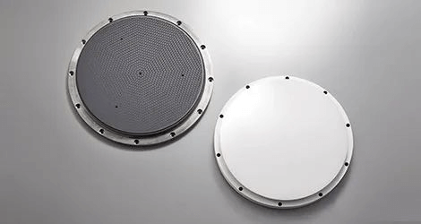
Ceramic electrostatic chuck
How do electrostatic chucks work?
Generally speaking, ceramic electrostatic chucks are mainly composed of three parts: a dielectric adsorption layer, an electrode layer and a base layer stacked from the surface to the inside in a layered structure. The dielectric adsorption layer is located on the surface to achieve efficient adsorption. The electrode layer is located in the middle. By applying positive or negative voltage, an electrostatic field is formed, and the base layer plays a supporting and fixing role. In addition, auxiliary structures such as electrode columns, gas channels, and bonding materials can also be embedded inside the electrostatic chuck. The gas can be introduced into the He gas during operation, and heat is transferred through the gas circulation flow, thereby stably controlling the temperature of the wafer. .
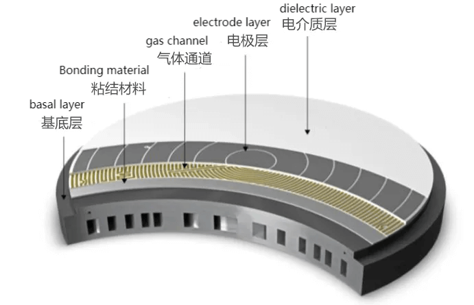
Electrostatic chuck structure
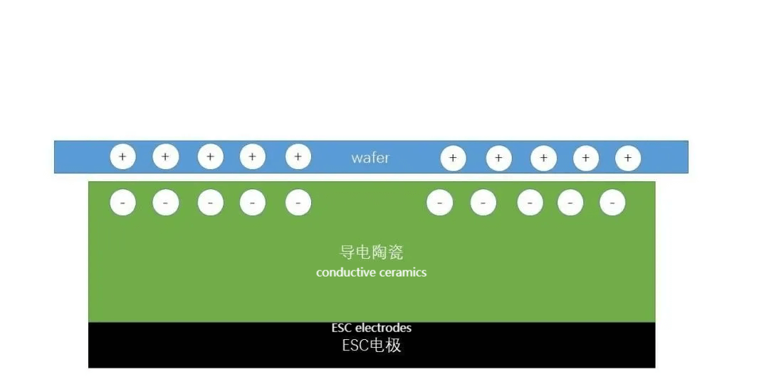
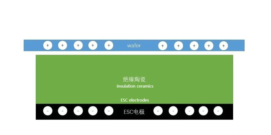
According to whether the dielectric adsorption layer is doped dielectric, electrostatic chucks can be divided into Coulomb type and JR type. The chucks made of pure dielectric (high resistance ceramic material) are Coulomb type, while those made of doped dielectric (such as doped dielectric) The suction cups made of ceramic materials mixed with titanium oxide (TO2) and other substances, which are semiconductors, are JR type. The adsorption principles of the two are quite different. They both use the electrostatic field formed in the electrode layer after the DC power supply is turned on to generate charges on the surface of the dielectric layer with opposite polarity to the charge on the surface of the wafer, thereby adsorbing the wafer. However, because the dielectric of the JR type electrostatic chuck has a certain conductivity, in addition to generating polarized charges, there is also a large part of free charges. Therefore, the suction force of the JR type electrostatic chuck is greater than that of the Coulomb type chuck, and it can achieve adsorption at a smaller voltage. However, during the desorption stage, due to the existence of free charges on the surface of the JR type sucker, in addition to turning off the high-voltage DC power supply, it is usually necessary to use reverse electrostatic voltage to forcefully eliminate the residual charges before the wafer can be desorbed, which increases the control to a certain extent. Difficulty and complexity.
The difference between Coulomb type and JR type electrostatic chuck
How are electrostatic chucks produced?
01 Material selection
Compared with metal materials, ceramic materials are not only wear-resistant and chip-free, avoiding the risk of chip contamination, but also have inherent advantages in electrical insulation. Therefore, electrostatic chuck technology mainly uses alumina ceramics or aluminum nitride ceramics as the main material. Generally speaking, for ordinary silicon wafer processing, high-purity aluminum oxide can be used as a material to meet the needs, but for silicon carbide wafer processing, an electrostatic chuck made of aluminum nitride is needed.
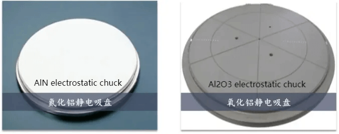
The thermal conductivity of aluminum nitride (theoretically up to 320W/(m·K)), matching with the thermal expansion coefficient of electrode materials, insulation and related mechanical properties are better than those of aluminum oxide. Not only can it be used in plasma halogen vacuum atmosphere It can operate for a long time and withstand the most demanding process environment of semiconductors and microelectronics. It can also provide more stable and sufficient adsorption force and better temperature control by controlling its volume resistivity. It is expected to gradually realize the electrostatic chuck of alumina ceramics. Substitution is the main development direction of electrostatic chucks in the future. However, in terms of the preparation process, due to the higher melting point of aluminum nitride and the small atomic self-diffusion coefficient, it is difficult to sinter and densify pure AlN ceramics. The sintering temperature is often required to be as high as 1800°C or above, which not only requires high sintering equipment, but also requires Selecting the appropriate sintering process, atmosphere and sintering aids to improve sintering performance is a complicated process.
02 Production route
Since the electrostatic chuck has at least one electrode embedded in a ceramic disk, in order to achieve one-time firing of the electrode material and the ceramic material, it is generally prepared using multi-layer ceramic co-firing technology, including casting, slicing, screen printing, and lamination. , hot pressing, sintering and other processes.
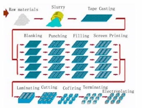
Multilayer co-fired ceramic technology flow chart
①Cast slicing:The dielectric layer of the Coulomb type electrostatic chuck is not doped with conductive materials. Ceramic powder, solvents, dispersants, binders, plasticizers, sintering aids and other ingredients can be mixed to prepare a stable slurry, which can then be cast on a casting machine. The ceramic green body of a certain thickness is obtained by scraper coating, drying and slicing. For the JR type electrostatic chuck, a certain amount of resistance adjusting agent (conductive material) needs to be added to increase the resistance of the J-R layer to the range required for the function, and then the green body is prepared by tape casting.
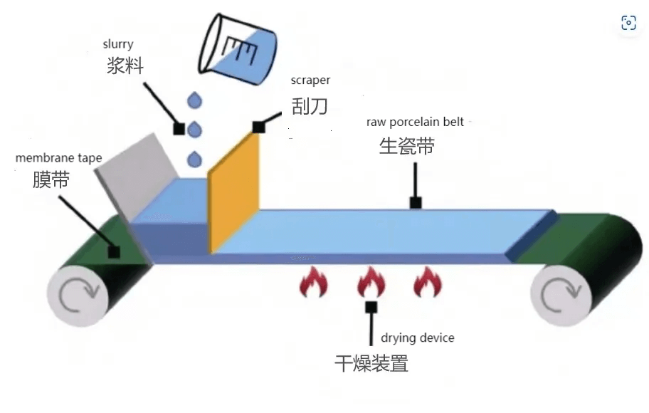
Casting machine
②Screen printing:
Screen printing is mainly used for the preparation of electrode layers. During the printing process, the conductive paste is first poured onto one end of the screen printing plate, and then under the action of the screen printing machine's scraper, the conductive paste is deposited on the substrate through the mesh of the screen printing plate. When printing After the scraper scrapes the entire screen printing plate and ensures that the silver paste fills the screen holes, a printing process can be completed.
③Lamination hot pressing:
The green porcelain sheets are stacked in the required order (base layer, electrode layer, dielectric layer) and number of layers at one time, and then the multiple layers of green porcelain sheets are connected together under specific temperature and pressure to form the required complete Green. It should be noted that during the lamination process, the pressure generated should be evenly distributed on the entire green body surface to ensure that the entire green body shrinks evenly after being pressed.
④Co-burning:
Finally, the complete green body is placed in the sintering furnace for integrated sintering. During this process, a suitable temperature rise and fall curve needs to be formulated to ensure flatness and shrinkage control during the sintering process. It is understood that Japan's NGK can control the shrinkage rate during powder sintering to about 10%, while the shrinkage rate of most domestic manufacturers is still greater than or equal to 20%.
Currently, in addition to the need to further develop higher purity, higher performance raw material ceramic powders and more efficient and stable production processes, it is also necessary to consider the needs of various specific application scenarios to optimize the structure design to meet the gradual increase in the size of the wafers. Large, increasing demand for temperature uniformity control.
Product page:https://www.ceramic-solutions.com/Boron-Nitride.html
Contact page:https://www.ceramic-solutions.com/Contact.html