Technical Article
Fluorine Plasma Etching: Why It Works and How Chamber Ceramics Resist It
Last reviewed: June 30, 2026
Contents
- Why fluorine plasma is used
- When fluorine is not the right chemistry
- How fluorine plasma etching works
- What the main gases do
- Why chamber components erode
- How to compare chamber ceramics
- How to select a material by component
- What to include in a ceramic RFQ
- Frequently asked questions
Fluorine plasma etching is widely used—not universally required—because fluorine radicals react with many silicon-based solids to form volatile fluorides. Those products can be pumped away, allowing controlled material removal. Ion bombardment can add directionality, while fluorocarbon fragments can passivate sidewalls and change selectivity.
The same reactive species and energetic ions also reach exposed chamber components. Over time, their combined action can roughen surfaces, change near-surface composition, and release particles. The practical question is not only “Why does fluorine etch the wafer?” but also “Which chamber material can tolerate this recipe without becoming a contamination source?”
The discussion connects fluorine chemistry with ceramic chamber components. It does not provide a process recipe, guarantee service life, or replace tool-specific qualification testing.
Why Is Fluorine Plasma Used in Dry Etching?
Plasma contains electrons, ions, neutral radicals, and molecular fragments. Electron-impact reactions dissociate feed gases such as CF4 or SF6 and generate reactive fluorine species. When those species reach a compatible solid, they can break surface bonds and form products with enough vapor pressure to leave the surface.
For silicon, a simplified reaction shorthand is:
Si(s) + 4F → SiF4(g)
The shorthand explains the main process advantage: silicon becomes gaseous silicon tetrafluoride rather than remaining as a non-volatile residue.
A review published by the French Academy of Sciences describes volatility as a first-order guide for choosing a halogen chemistry. Fluorine readily etches many group-14 materials, including silicon and germanium, while chlorine or bromine may be more suitable for other materials and profile requirements. The same review notes that SF6 can produce a high fluorine-atom concentration for efficient silicon removal. Read the fluorine-plasma review.
Does All Dry Etching Require Fluorine Plasma?
No. “Dry etching” describes material removal without a liquid etchant; it is broader than fluorine plasma etching.
Arizona State University lists fluorine, chlorine, methane/hydrogen, and oxygen among its available plasma chemistries. It also operates a XeF2 vapor-phase silicon etcher that does not use plasma. The correct chemistry depends on whether the target material can form a removable reaction product and whether the process needs a particular etch rate, profile, mask selectivity, or stopping layer. See ASU's dry-etch process guide.
Important boundaries include:
- Silicon, SiO2, and Si3N4: Fluorine and fluorocarbon chemistries are common.
- Many compound semiconductors and metals: Chlorine- or bromine-based chemistries may provide better product volatility or profile control.
- Photoresist removal: Oxygen plasma is widely used.
- Isotropic silicon release: XeF2 vapor can etch silicon without sustaining a plasma in the process chamber.
This distinction matters for material selection. A ceramic that performs well in a fluorine-rich recipe may behave differently under Cl2, BCl3, HBr, oxygen, or mixed-gas exposure.
How Fluorine Plasma Etching Works
The wafer surface is removed through a balance of three effects.
1. Chemical Reaction
Neutral fluorine radicals adsorb on the surface and form fluorinated products. Chemical removal can be fast but relatively isotropic because neutral species arrive from many directions.
2. Ion-Assisted Removal
Positive ions accelerate across the plasma sheath toward a biased surface. Their momentum can break bonds, remove passivation from horizontal surfaces, and help reaction products desorb. Directional ion flux is one reason reactive ion etching can create more anisotropic profiles than neutral-radical etching alone.
3. Fluorocarbon Deposition and Passivation
Carbon-containing feed gases also generate CFx fragments. These fragments can deposit a fluorocarbon-rich film. Ion bombardment removes that film more readily from horizontal surfaces than protected sidewalls, allowing vertical etching while suppressing lateral attack.
The fluorine-to-carbon, or F/C, concept describes this competition. A fluorine-rich plasma tends to favor chemical removal; a carbon-rich plasma tends to favor polymer deposition. It is a process trend, not a stand-alone recipe rule. Power, pressure, gas flow, bias, temperature, chamber condition, and target material all change the result.
What Do CF4, SF6, C4F8, CHF3, and NF3 Do?
| Gas | Main Process Role | Typical Use | Material-Selection Implication |
|---|---|---|---|
| CF4 | Fluorine source plus CFx fragments | Si, SiO2, and Si3N4 etching; often mixed with O2 or other gases | Exposed parts face both fluorination and fluorocarbon deposition; surface condition can change over a maintenance cycle |
| SF6 | High fluorine-radical source | Fast silicon etching and the etch step of the Bosch DRIE process | High fluorine exposure can accelerate chemical attack on unsuitable chamber surfaces |
| C4F8 | Strong fluorocarbon-film former | Sidewall passivation in Bosch DRIE and other profile-control schemes | Deposited films can protect some areas but also alter particle adhesion and cleaning requirements |
| CHF3 | Fluorine source with stronger polymer-forming tendency than CF4 | Dielectric etching where selectivity and profile control matter | Component behavior depends on the balance between polymer coverage, ion removal, and fluorine exposure |
| NF3 | Efficient remote-plasma fluorine source | Cleaning silicon-containing deposits from CVD and related chambers | Chamber-cleaning exposure is not the same as patterned-wafer etching; remote radicals and the cleaned deposit must be considered |
NF3 deserves separate treatment. It is commonly dissociated in a remote plasma source so reactive fluorine reaches deposited material in a chamber without using NF3 as the patterned-wafer etchant. A U.S. National Institute of Standards and Technology environmental filing describes NF3 remote cleaning as distinct from wafer processing. See the NIST project filing.
Why Fluorine Plasma Also Attacks Chamber Components
Etching species do not interact only with the intended wafer area. Chamber walls, liners, rings, gas-distribution parts, and insulators may receive neutral-radical flux, ion flux, or both. Four damage routes matter:
- Chemical fluorination: Surface atoms react with fluorine and form a fluoride or oxyfluoride layer.
- Ion sputtering: Energetic ions remove atoms or weakly bonded reaction layers.
- Surface roughening: Grain boundaries, pores, and phase differences can etch at different rates.
- Particle generation: Reaction layers, redeposited process films, or weakened grains can detach and reach the wafer.
These routes interact. Ion bombardment may remove a protective fluoride layer, while pores, cracks, or weak coating interfaces create local attack sites. Particle performance therefore cannot be inferred from bulk chemistry alone.
Peer-reviewed studies support this microstructure-sensitive view. One YF3 film experiment used 800 W source power, 100 W bias, 3 mTorr pressure, 25 sccm CF4, 5 sccm O2, and 10–30 minute exposures; its measured etching depth was three times lower than an Al2O3 reference. A separate Y2O3-MgO study linked plasma resistance to grain size, density, and mechanical reliability. These values are evidence from stated tests, not universal design rules. Review the YF3 film study and the Y2O3-MgO ceramic study.
How to Compare Plasma-Resistant Ceramics
| Candidate Material | Potential Strengths | Important Limits | Where to Investigate It |
|---|---|---|---|
| Y2O3 / yttria | Low erosion and stable fluorinated surface layers in many fluorine-plasma studies; high-purity options can reduce metal contamination | Brittleness, porosity, grain structure, coating adhesion, and cost require review | Liners, rings, nozzles, coatings, and other directly exposed components |
| Al2O3 / alumina | Established supply base, electrical insulation, mechanical strength, and broad shape capability | Some fluorine-rich conditions can produce more erosion or particle release than dense yttria systems | Insulators, windows, structural parts, and lower-exposure zones where cost and mechanical needs matter |
| CVD-SiC | High purity, thermal conductivity, and dimensional stability; electrical behavior may suit selected plasma-facing parts | Conductivity, joining, fabrication route, cost, and exact plasma chemistry must match the tool | Focus rings and thermally loaded components after electrical and contamination review |
| Si3N4 | High mechanical strength, fracture resistance, and useful electrical properties | Silicon nitride is itself etched by many fluorine chemistries, so it is not a default choice for a directly exposed high-flux surface | Mechanically loaded or shielded parts where plasma exposure is limited and electrical function dominates |
| YAG and related yttrium-aluminum ceramics | Research indicates a useful balance of plasma behavior and mechanical properties in selected conditions | Performance depends on phase composition, density, and recipe; less direct production history may be available | Application-specific alternatives when pure yttria's mechanical or manufacturing limits matter |
Plasma resistance is a system property, not a single material constant.
Gas mix, dissociation, ion energy, temperature, chamber position, surface finish, density, porosity, and previous cleaning history all influence component behavior.
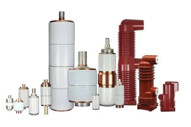
Cersol's Y2O3 ceramic page describes high-purity bulk and coating options for semiconductor equipment. Its ceramic focus ring page identifies yttria and CVD-SiC as candidate materials for customized rings. These pages are starting points for an engineering review, not substitutes for tool-specific qualification.
Component-to-Material Selection Matrix
| Component | Main Concerns | Candidate Starting Points | Questions Before Selection |
|---|---|---|---|
| Chamber liner or wall coating | Large exposed area, particle shedding, coating adhesion, maintenance cleaning | Dense Y2O3 coating or bulk yttria; alumina where exposure and cost allow | Is the dominant flux radical or ion driven? What cleaning sequence follows the process? |
| Focus ring | Edge-plasma interaction, dimensional stability, electrical coupling, particle control | Y2O3 or CVD-SiC depending on electrical and thermal requirements | Must the ring be insulating, semiconductive, or conductive? Which surfaces see direct bias-driven ions? |
| Showerhead or gas nozzle | Gas distribution, local erosion, hole geometry, contamination, and thermal cycling | High-purity Y2O3, alumina, or another qualified ceramic | Are the holes exposed to direct plasma? What dimensional change is acceptable before replacement? |
| Window or insulating spacer | Dielectric strength, thermal shock, optical/RF function, and edge exposure | Alumina or yttria, selected by exposure level and functional requirement | Does the part transmit RF or light? Are edges shielded from direct ion bombardment? |
Engineering Data to Include in a Ceramic RFQ
A useful request for quotation should describe the operating system rather than naming a material alone. Include:
- Gas chemistry and approximate flow ratios
- Plasma source type: capacitively coupled, inductively coupled, or remote plasma
- Source power, bias power, or expected ion-energy range
- Pressure and operating-temperature range
- Component position and surfaces directly exposed to plasma
- Electrical requirement: insulating, semiconductive, or conductive
- Purity and allowable contaminant elements
- Surface-finish and dimensional-tolerance requirements
- Drawing, quantity, and joining or coating interfaces
- Current material, observed failure mode, and replacement interval
- Cleaning chemistry and maintenance sequence
Fluorine plasma is common in dry etching because reactive fluorine can convert many silicon-based materials into volatile products, while ions and fluorocarbon films help control directionality and selectivity. That same environment exposes chamber components to fluorination, sputtering, roughening, and particle-generation risk.
The right ceramic is selected by the full exposure condition, not by a gas name or a single published etch-rate value. Start with the target material, plasma source, bias, temperature, component function, and contamination limit; then compare candidate yttria, alumina, CVD-SiC, silicon nitride, or yttrium-aluminum systems under representative conditions.
This approach turns a broad material list into a qualification plan: define the exposure, match the component's electrical and thermal function, test the candidate under representative conditions, and set a measurable replacement criterion before production release.
Frequently Asked Questions
Need custom plasma-resistant ceramic component support?
Contact Our TeamEngineering References
- D. Cardinaud et al., “Fluorine-based plasmas: Main features and application in micro- and nanotechnology and in surface treatment,” Comptes Rendus Chimie, 2018. https://doi.org/10.1016/j.crci.2018.01.009
- Arizona State University Core Research Facilities, “Techniques—Dry Etch,” accessed June 29, 2026. View the university process guide.
- W.-K. Wang, Y.-X. Lin, and Y.-J. Xu, “Structural and Fluorine Plasma Etching Behavior of Sputter-Deposition Yttrium Fluoride Film,” Nanomaterials, 2018. https://doi.org/10.3390/nano8110936
- H.-M. Oh et al., “Remarkable plasma-resistance performance by nanocrystalline Y2O3-MgO composite ceramics for semiconductor industry applications,” Scientific Reports, 2021. https://doi.org/10.1038/s41598-021-89664-9
- U.S. National Institute of Standards and Technology, Micron Semiconductor Manufacturing Project—Final Environmental Impact Statement, Appendices H–J, 2025. View the NIST filing.