Technical Article
Wafer Thinning and Semiconductor Ceramic Tooling Guide
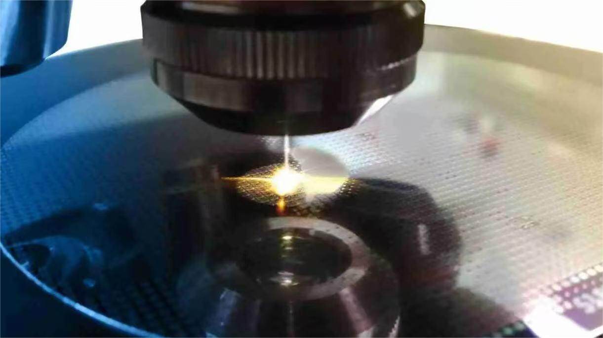
Wafer thinning is the controlled removal of material from the backside of a semiconductor wafer to reduce thickness, improve thermal performance, enable advanced packaging and prepare the wafer for dicing, stacking or bonding. In production, the process connects backside grinding, polishing, stress relief, wafer handling, cleaning and metrology, and it often depends on stable semiconductor ceramic tooling to reduce nonuniform vacuum support, particle contamination, carrier flatness errors and rough wafer transfer.
What Is Wafer Thinning?
Wafer thinning is the backside removal of silicon, silicon carbide, gallium arsenide, sapphire, glass or another wafer material after front-side device fabrication or before advanced packaging. The objective is to reach a specified final thickness while preserving device performance, wafer flatness and mechanical strength. A thinned wafer may later be diced, stacked, bonded, metallized or mounted into a package.
In many process flows, thinning is not a single operation. A wafer may be mounted on protective tape, ground in two stages, polished or etched to remove damage, cleaned, measured, inspected and then diced. For ultra-thin work, the wafer may be temporarily bonded to a carrier so it can survive handling below ordinary free-standing thickness limits.
Definition for quick reference: Wafer thinning is a semiconductor manufacturing step that reduces wafer thickness from the backside through grinding, polishing, lapping, etching or related processes. It is used to lower package height, improve heat dissipation, expose through-silicon vias, increase flexibility and prepare wafers for dicing, stacking or temporary bonding workflows.
Why Are Semiconductor Wafers Thinned?
Wafers are thick enough to survive crystal growth, slicing, polishing, lithography, deposition and handling. A production wafer must be rigid during front-end processing, but the final device often needs to be much thinner. Backside thinning bridges that gap between process robustness and package performance.
| Goal | Why It Matters | Typical Process Concerns |
|---|---|---|
| Reduce package height | Thin packages are needed for mobile, sensor, memory and stacked devices. | Final thickness, breakage risk and edge chipping. |
| Improve heat dissipation | Shorter thermal paths can help power devices transfer heat into the package or heat spreader. | Backside roughness, stress, metallization compatibility and flatness. |
| Enable 3D integration | Stacked die, TSV and wafer-level packaging often need a reduced substrate thickness. | Temporary bonding, TSV reveal depth, TTV and debond cleanliness. |
| Improve electrical or RF behavior | Some RF, MEMS and sensor devices require controlled substrate thickness. | Uniformity, surface damage and device-side protection. |
| Prepare for singulation | Thinner wafers reduce dicing load and package profile. | DBG, SDBG, tape choice, kerf quality and die edge strength. |
A simple thickness target is not enough. A wafer thinned to the right average thickness can still fail if total thickness variation is high, if grinding cracks remain in the backside, or if excessive bow creates downstream alignment problems. That is why mature wafer thinning specifications include both dimensional and damage-related controls.
Standard Wafer Thinning Process Flow
A typical thinning route uses a high-removal step first and a low-damage finishing step later. The exact sequence depends on wafer material, final thickness, front-side topology, acceptable damage depth and whether the wafer will be diced before or after grinding.
- Incoming inspection: confirm wafer diameter, starting thickness, notch or flat orientation, front-side sensitivity, existing bow, contamination limits and edge condition.
- Front-side protection: apply UV tape, protective tape, coating or temporary bonding to a carrier to protect devices and support thin wafers.
- Coarse backgrinding: remove bulk material at a high removal rate using a diamond wheel or equivalent abrasive process.
- Fine grinding: reduce grinding marks and approach the target thickness with a finer grit, lower load and tighter thickness control.
- Stress relief: remove or reduce subsurface damage using polishing, CMP, dry polishing, wet etching, plasma etching or another low-damage process.
- Cleaning and drying: remove grinding debris, slurry, tape residue and particles without attacking the front-side devices.
- Metrology: measure final thickness, total thickness variation, bow, warp, surface roughness and sometimes residual stress or die strength.
- Downstream processing: proceed to dicing, dicing-before-grinding, backside metallization, wafer bonding, TSV reveal, inspection or packaging.
The most common production sequence for silicon is coarse grind, fine grind and backside stress relief. However, ultra-thin wafers, compound semiconductors and hard materials such as SiC often require modified wheels, chemical assistance, plasma methods, carrier support or special dicing integration.
Where Semiconductor Ceramic Components Fit in Wafer Thinning
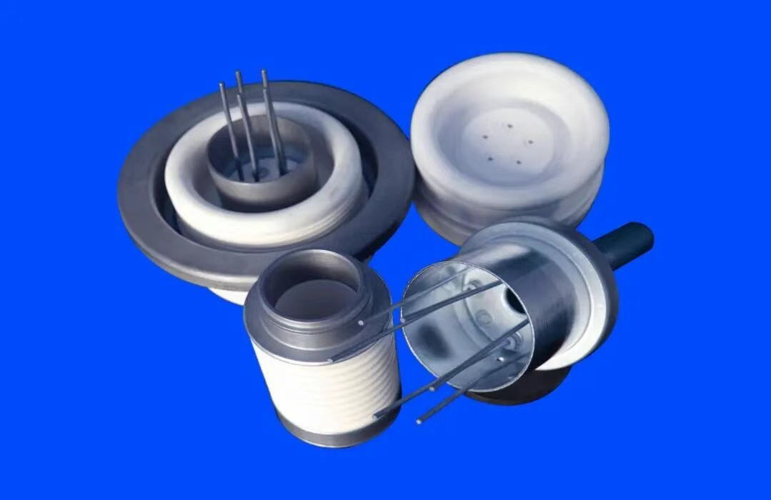
The commercial bridge between wafer thinning and semiconductor ceramics is not the silicon removal itself. It is the ceramic tooling that holds, supports, transfers, polishes, heats or protects wafers before and after thinning. Thin wafers are sensitive to local suction marks, particles, vibration, thermal drift and edge stress, so ceramic materials such as alumina, porous alumina, silicon carbide, aluminum nitride and yttria-stabilized ceramics are often selected for stiffness, cleanliness, wear resistance, chemical stability and dimensional control.
| Wafer Thinning Need | Relevant Semiconductor Ceramic Component | Common RFQ Wording |
|---|---|---|
| Uniform vacuum support for thin wafers during grinding, dicing, cleaning or inspection. | Wafer porous chuck and wafer vacuum chuck. | porous ceramic vacuum chuck, wafer porous chuck, ceramic vacuum chuck, porous alumina chuck, SiC vacuum chuck. |
| Stable wafer transfer between thinning, CMP, metrology and dicing modules. | Wafer end effector and ceramic wafer handler. | ceramic end effector, ceramic robot blade, wafer handling arm, ceramic wafer handler, vacuum wand. |
| Backside smoothing, lapping or CMP after grinding damage removal. | CMP alumina polishing plate and precision lapping/polishing ceramic fixtures. | CMP polishing plate, alumina polishing plate, ceramic lapping plate, semiconductor polishing fixture. |
| Thermal stability for adjacent deposition, annealing, bonding or test steps. | AlN heater and aluminum nitride ceramic heating components. | AlN heater, aluminum nitride ceramic, semiconductor heater, ceramic heater plate. |
| Plasma, etch or chamber-adjacent environments used before or after thinning. | Ceramic focus ring, yttria ceramic and silicon carbide ceramic parts. | ceramic focus ring, Y2O3 ceramic, yttria ceramics, silicon carbide ceramic parts, plasma resistant ceramic. |
In practical purchasing, wafer thinning problems often become ceramic tooling questions. When TTV, wafer bow, backside damage or thin-wafer handling is the issue, the component choice may involve a ceramic chuck, carrier, robot blade, polishing plate or custom ceramic fixture that supports the wafer without adding particles, deformation or mechanical damage.
Wafer Thinning Methods Compared
SERP results for wafer thinning usually mention grinding, lapping, polishing and etching, but those methods are not interchangeable. The right method depends on whether the priority is removal speed, surface quality, flatness, damage removal, material compatibility or cost.
| Method | Best Use | Strengths | Limitations |
|---|---|---|---|
| Backgrinding | Bulk thickness removal from silicon and many compound semiconductor wafers. | Fast, scalable and widely used for production thinning. | Leaves grinding marks and subsurface damage unless followed by stress relief. |
| Fine grinding | Approaching final thickness after coarse removal. | Improves thickness control and reduces damage compared with coarse grinding. | May still require polishing, dry polishing or etching for strength-sensitive devices. |
| Lapping | Flatness correction and material removal where two-sided control is useful. | Can improve flatness and process difficult materials. | Usually slower and less clean than modern grinding/polishing flows. |
| CMP | Backside smoothing, damage reduction and tight surface finish requirements. | Combines chemical and mechanical action for lower-damage surfaces. | Lower removal rate and more slurry/cleaning control than grinding. |
| Dry polishing | Post-grind stress relief without slurry in selected processes. | Can improve die strength and reduce wet chemical handling. | Process window depends on wheel, wafer material and required roughness. |
| Wet etching | Removing a damaged layer after grinding. | Can remove microcracks without mechanical contact. | Chemical compatibility, isotropy, waste handling and uniformity need control. |
| Plasma etching or atmospheric downstream plasma | Damage removal, SiC processing and low-contact finishing routes. | Useful where mechanical damage must be minimized or hard materials are difficult to grind. | Tooling, chemistry, selectivity and throughput must match the application. |
Industrial wafer thinning routes commonly combine mechanical grinding, chemical-mechanical polishing, wet etching or plasma-based finishing depending on material, target thickness and surface requirement. Tooling and process recipes may also separate grinding, polishing, TAIKO-style rim support, DBG/SDBG and in-line thickness control as distinct routes for different thinning challenges.
Critical Process Controls: TTV, Bow, Warp and Surface Damage
A good wafer thinning process is measured by more than final thickness. The wafer must remain usable in downstream lithography, bonding, dicing, die attach or packaging. The most important control metrics are listed below.
- Final thickness: the average wafer thickness after thinning and finishing.
- Total thickness variation: the difference between the thickest and thinnest points across the wafer or specified measurement area.
- Bow and warp: out-of-plane deformation that can affect handling, alignment, bonding and chucking.
- Surface roughness: the micro-scale texture of the backside after grinding, polishing or etching.
- Subsurface damage: cracks and strained material below the visible surface, often created by abrasive grinding.
- Die strength: mechanical resistance of the thinned die after singulation, especially important for thin and large die.
- Particles and residues: contamination from grinding debris, slurry, tape adhesive, chemicals or carrier bonding materials.
In-line metrology is valuable because waiting until final inspection can waste wafers. Some grinding systems measure wafer thickness before, during and after grinding so the process can be adjusted before a wafer drifts out of tolerance. The broader lesson is simple: thickness control should be part of the process loop, not only a final certificate.
Engineering note: If the buyer only specifies "thin to 100 µm," the supplier may meet the average thickness while leaving unacceptable TTV, bow or grinding damage. A complete specification should define thickness tolerance, measurement map, backside finish, edge exclusion, chipping limit and inspection method.
Ultra-Thin Wafer Handling: Temporary Bonding, TAIKO and DBG
Once wafers approach ultra-thin thickness ranges, mechanical handling becomes the central risk. Thin wafers flex, crack, warp and break more easily. Device wafers also have front-side structures that cannot be scratched, contaminated or loaded unevenly. Three approaches appear repeatedly in top-ranking technical pages and vendor resources: temporary bonding, TAIKO grinding and dicing-before-grinding.
Temporary Bonding and Debonding
Temporary bonding attaches the device wafer to a carrier wafer with an adhesive or bonding layer so the thin wafer can be ground, polished, etched or otherwise processed without free-standing breakage. After backside work is complete, the wafer is debonded and cleaned. This route is common when very thin or fragile wafers must pass through backgrinding, backside processing and debonding steps.
Temporary bonding specifications should include carrier material, adhesive chemistry, maximum thermal budget, topography tolerance, debond method, residue limits and post-debond cleaning. These details are especially important for TSV reveal, wafer-level packaging, MEMS and compound semiconductor devices.
TAIKO Grinding
TAIKO grinding thins the inner portion of the wafer while leaving a thicker outer rim. The rim helps preserve stiffness during handling and transport, which can reduce handling risk and backside chipping when wafers become very thin.
Dicing Before Grinding and SDBG
Dicing before grinding changes the order of operations. Grooves are formed from the front side before thinning, then backside grinding reaches those grooves and separates the die. In suitable flows, this approach can reduce die edge chipping and improve thin die handling. It is not a universal replacement for conventional dicing, but it is important when thin die edge strength is a high-priority requirement.
Material-Specific Wafer Thinning Considerations
Different wafer materials respond differently to grinding, polishing and etching. Silicon is the reference case, but compound semiconductors, SiC, sapphire and glass require process changes because hardness, brittleness, thermal conductivity, chemistry and device structures vary.
| Material | Typical Concern | Process Implication |
|---|---|---|
| Silicon | Mature process, but damage and TTV still affect die strength and assembly yield. | Coarse/fine grinding plus stress relief is common. |
| Silicon carbide | High hardness and slow mechanical removal. | Requires optimized diamond tooling, low-damage finishing or plasma-assisted routes. |
| GaAs, InP and other compound semiconductors | Brittleness, toxicity concerns and device sensitivity. | Gentle handling, protective bonding and controlled cleaning are critical. |
| Sapphire and glass | Hard, brittle materials with edge and crack sensitivity. | Wheel selection, edge support and polishing sequence matter. |
| MEMS and sensor wafers | Front-side topography, cavities or fragile membranes. | Temporary bonding, pressure control and custom fixtures may be needed. |
Ceramic tooling also matters in thinning workflows. Porous ceramic vacuum chucks, ceramic carriers and precision lapping or polishing consumables help stabilize wafers during processing. For related component support, Ceramic-Solutions provides wafer porous chucks, wafer vacuum chucks, CMP alumina polishing plates and broader semiconductor ceramic components used around wafer handling and precision processing environments.
Common Wafer Thinning Defects and How to Reduce Them
Most thinning failures come from a mismatch between the wafer, the abrasive process and the downstream requirement. The defect may be visible immediately, or it may appear later as die breakage, package cracking, poor bonding or electrical yield loss.
| Defect | Likely Causes | Reduction Strategy |
|---|---|---|
| Subsurface microcracks | Aggressive coarse grind, unsuitable wheel, high load or poor coolant control. | Use fine grind and stress relief; verify with die strength or surface analysis. |
| High TTV | Chuck flatness, tape nonuniformity, carrier issues or unstable grind control. | Improve mounting, chuck condition, in-line thickness control and measurement map. |
| Wafer bow or warp | Residual stress, front-side films, asymmetric removal or thermal mismatch. | Add stress relief, balance film stack, use carrier support and control thermal steps. |
| Edge chipping | Edge contact, weak bevel, abrasive overload or dicing interaction. | Consider edge trimming, TAIKO, DBG/SDBG or optimized dicing tape and parameters. |
| Particle contamination | Grinding debris, slurry residue, tape adhesive or inadequate cleaning. | Specify cleaning chemistry, particle inspection and residue limits after debond. |
| Front-side damage | Poor tape, bonding voids, pressure marks or chemical exposure. | Validate protection stack, carrier bonding uniformity and debond process. |
How Thin Can a Wafer Be?
There is no universal minimum thickness because wafer diameter, material, device layout, front-side films, carrier support and downstream handling all matter. Many silicon wafer thinning services commonly support final thicknesses in the tens of microns, while ultra-thin development can go lower under tightly controlled conditions. Very low single-digit micrometer examples exist for selected 300 mm silicon wafers, but such results depend on specialized process conditions and are not ordinary commodity thinning.
For commercial RFQs, it is better to specify the actual device need instead of asking for the thinnest possible wafer. A target such as 100 µm with controlled TTV, low backside damage and proven die strength may produce better yield than forcing a 50 µm target that increases breakage and handling cost without improving package performance.
Supplier Checklist for Wafer Thinning and Semiconductor Ceramic Tooling
A good wafer thinning RFQ should make the process risk visible before the quotation stage. If the project involves semiconductor ceramic tooling, include both wafer-process data and ceramic-component data so the supplier can recommend the right porous ceramic chuck, ceramic wafer carrier, end effector, polishing plate or custom fixture.
RFQ worksheet
- Wafer material: silicon, SiC, GaAs, InP, sapphire, glass or another material.
- Wafer size: 2 in, 3 in, 4 in, 6 in, 8 in, 12 in or custom diameter.
- Starting thickness, final thickness and thickness tolerance.
- Required TTV, bow, warp, surface roughness and measurement method.
- Front-side device status, topography height and protection requirement.
- Temporary bonding, carrier, tape or coating requirements.
- Backside finish: ground, fine ground, polished, CMP, etched or stress relieved.
- Downstream process: dicing, DBG, bonding, metallization, die attach, TSV reveal or packaging.
- Allowed edge exclusion, chipping limit and die edge quality requirement.
- Cleanliness: particle limit, ionic contamination, organic residue and packaging method.
- Inspection data: thickness map, microscope images, roughness data, bow/warp report or die strength test.
- Lot size, sample quantity, production volume and traceability requirements.
- Ceramic tooling type: porous vacuum chuck, wafer porous chuck, ceramic carrier, ceramic end effector, ceramic wafer handler, CMP polishing plate or custom fixture.
- Ceramic material preference: alumina, porous alumina, silicon carbide, aluminum nitride, yttria ceramic or application-specific advanced ceramic.
- Tooling specifications: pore size, porosity, flatness, surface roughness, vacuum pattern, contact area, cleanroom class, ESD requirement and chemical exposure.
Ceramic-Solutions supports semiconductor manufacturing environments with precision ceramic parts used around wafer handling, grinding, polishing and high-cleanliness processes. If your thinning workflow needs porous ceramic vacuum chucks, wafer porous chucks, ceramic wafer handlers, end effectors, lapping plates, CMP polishing plates or custom fixtures, share the wafer size, flatness target, vacuum pattern, material requirement and operating environment with the engineering team.
Conclusion
Wafer thinning is not only a backside material removal step. It is a yield-sensitive process that connects front-side device protection, grinding, polishing, stress relief, cleaning, metrology and downstream packaging. The best process is the one that reaches the target thickness while preserving die strength, flatness, surface quality and cleanliness.
For robust results, define more than final thickness. Specify TTV, bow, warp, roughness, damage control, temporary bonding needs, dicing method and inspection data. When the wafer thinning workflow depends on stable ceramic tooling or precision semiconductor ceramic parts, Ceramic-Solutions can support porous alumina and SiC vacuum chucks, wafer porous chucks, ceramic carriers, ceramic wafer handlers, end effectors, alumina CMP polishing plates and related custom fixtures.
FAQ
Need porous ceramic vacuum chucks, wafer porous chucks, ceramic wafer handlers, CMP alumina polishing plates or custom semiconductor ceramic tooling for wafer thinning and semiconductor processing?
Contact Our Team