19-January-2026
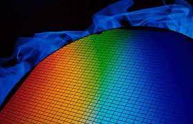
In the world of advanced electronics, the ability to build materials one atomic layer at a time is the ultimate superpower. Metal-Organic Chemical Vapor Deposition, universally known as MOCVD, is the primary technology that makes this possible. MOCVD is a sophisticated manufacturing process used to "grow" high-quality crystalline layers onto a semiconductor wafer. Instead of using liquid melts or solid blocks, MOCVD uses gases to transport atoms, allowing for the creation of complex sandwich-like structures that power modern life. From the screen on your phone to the sensors in autonomous cars, MOCVD is the invisible force shaping the digital age.
The magic of MOCVD lies in its specialized starting materials, known as precursors. These are "metal-organic" molecules—essentially metal atoms like Gallium or Indium tucked inside organic "delivery trucks" made of carbon and hydrogen. In a MOCVD system, these precursors are turned into a vapor and mixed with other gases. This gaseous mixture is then precisely metered into a reaction chamber. Because the atoms are carried in a gas, MOCVD allows for extreme control, enabling engineers to switch materials on and off in a fraction of a second to create interfaces that are perfectly flat at the atomic level.
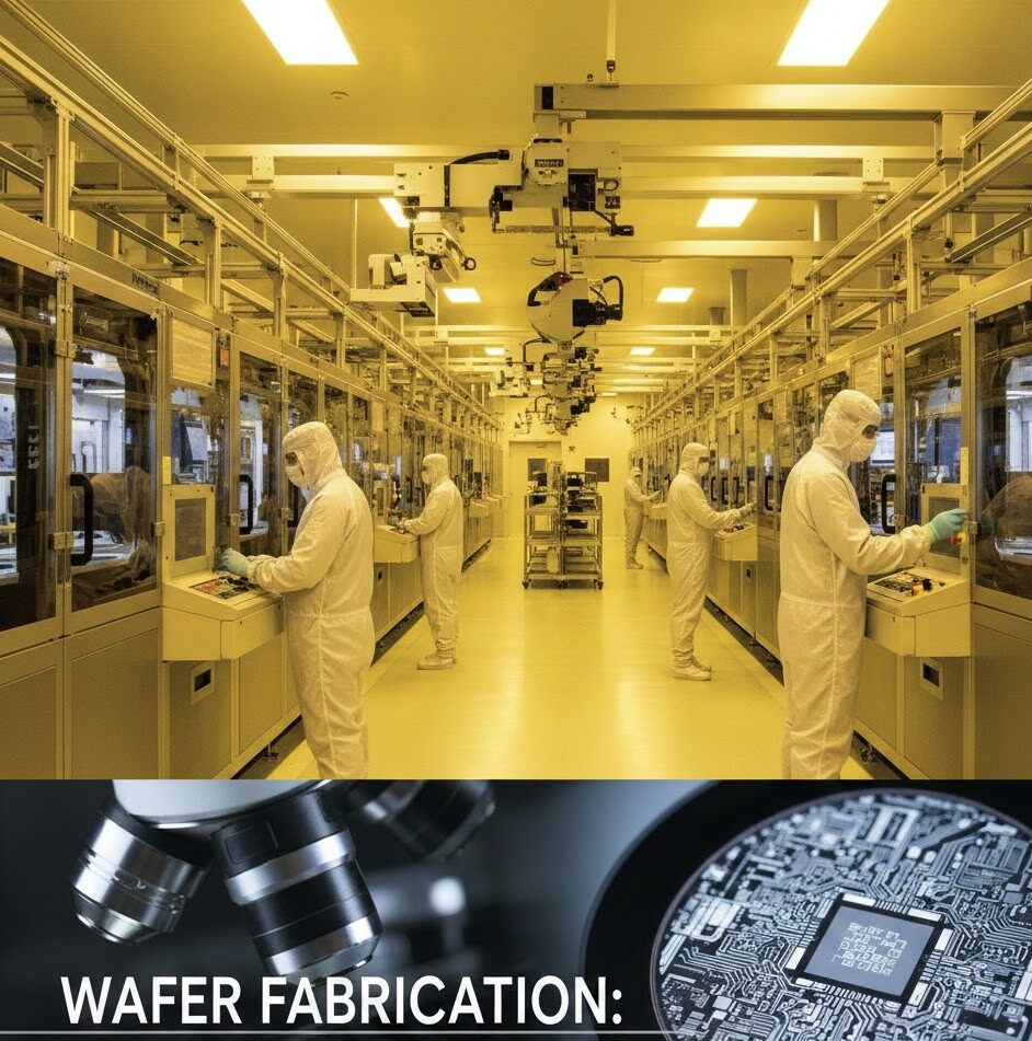
Inside the MOCVD Reactor
The heart of the MOCVD process is the reactor, a chamber designed to handle extreme heat and highly pure chemicals. Inside, the semiconductor wafer sits on a platform called a susceptor, which is heated to intense temperatures, often exceeding 1,000 degrees Celsius. The design of the MOCVD reactor ensures that the gas flows smoothly and evenly across the wafer surface. Precision is everything in an MOCVD reactor; even a tiny fluctuation in temperature or gas flow can ruin the performance of the resulting chip. Modern MOCVD systems are highly automated, capable of processing dozens of wafers at once to meet global demand.
The Boundary Layer
One of the most critical scientific concepts in MOCVD is the "boundary layer." As the precursor gases flow through the MOCVD chamber, they encounter a thin, stagnant layer of gas hovering just above the hot wafer. To form a crystal, the metal-organic molecules must diffuse through this MOCVD boundary layer. Engineers carefully tune the pressure and flow speed inside the MOCVD reactor to keep this layer consistent. By mastering this invisible barrier, MOCVD can produce films that are incredibly uniform in thickness across the entire surface, which is essential for mass-producing millions of identical chips.
Pyrolysis
When the precursor molecules finally reach the hot wafer surface, they undergo a chemical transformation called pyrolysis. The intense heat of the MOCVD process breaks the chemical bonds of the metal-organic "delivery trucks," releasing the metal atoms. These atoms then settle onto the surface and arrange themselves into a perfect crystal lattice, following the pattern of the wafer beneath them. Meanwhile, the organic remnants are swept away as waste gas. This continuous cycle of delivery, decomposition, and arrangement allows MOCVD to build up materials layer by layer with surgical precision.
Technically, MOCVD has emerged as the "workhorse" of the industry because it strikes a perfect balance between speed and quality. While other techniques might offer more extreme vacuum conditions, MOCVD is prized for its high growth rates and scalability. It is particularly effective at growing "III-V" compound semiconductors—materials that combine elements like Gallium and Nitrogen. Over the decades, MOCVD technology has evolved from small laboratory setups into massive industrial tools. Today, the ability of MOCVD to deliver consistent, high-purity materials at a fast pace makes it the dominant choice for large-scale commercial manufacturing.
MOCVD and the LED Revolution
The most famous application of MOCVD is the production of Light Emitting Diodes (LEDs). Every blue and white LED used in modern lighting was likely grown in an MOCVD reactor. By precisely layering different semiconductors, MOCVD allows for the creation of "quantum wells" that turn electricity into light with incredible efficiency. Currently, MOCVD is at the center of the MicroLED revolution, which aims to create next-generation displays for smartwatches and AR glasses. These displays require thousands of microscopic LEDs per square inch, a feat that only the atomic-level precision of MOCVD can achieve.
Lasers and Optical Communication
MOCVD is also the engine behind the global internet infrastructure. The laser diodes that send data through thousands of miles of fiber-optic cables are manufactured using MOCVD. These lasers require extremely complex "heterostructures" where the material composition changes multiple times over a few nanometers. MOCVD is the only technology capable of producing these structures with the necessary reliability for telecommunications. Furthermore, the VCSEL sensors used for facial recognition in smartphones are direct products of MOCVD growth, proving that this technology is literally looking back at us every day.
MOCVD in Power Electronics
As the world shifts toward electric vehicles (EVs) and renewable energy, MOCVD is taking on a new role in power electronics. Traditional silicon chips are being replaced by Gallium Nitride (GaN) and Silicon Carbide (SiC) chips, which can handle higher voltages and run much cooler. MOCVD is the essential tool for growing the thin layers of GaN needed for fast-charging bricks and EV power inverters. By using MOCVD to create these high-performance materials, we can charge our phones in minutes and extend the range of electric cars, making green technology more practical for everyone.
The 6G Frontier
Looking toward 2025 and 2030, MOCVD research is pushing into the realm of 6G communications and ultra-wide bandgap materials. Scientists are using MOCVD to explore new materials like Gallium Oxide, which can handle even more power than today’s best semiconductors. As we move toward a world of 6G connectivity, MOCVD will be used to build the high-frequency chips that will make near-instant data transmission a reality. The MOCVD reactor remains the ultimate tool for atomic engineering, turning invisible vapors into the solid foundation of our technological future.