26-January-2026
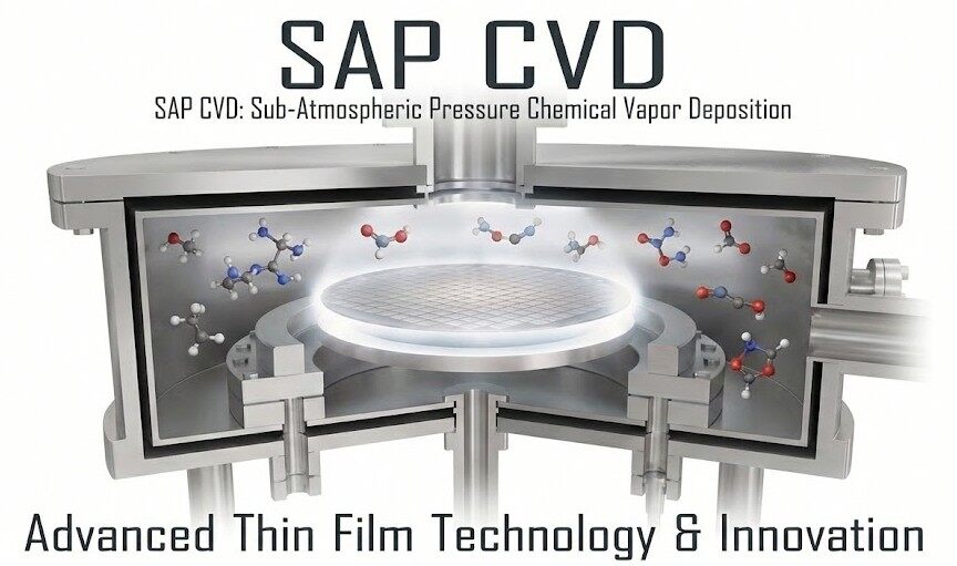
High Density Plasma Chemical Vapor Deposition, usually shortened to HDPCVD, is a thin-film deposition technology widely used in advanced semiconductor manufacturing. HDPCVD is especially famous for one thing: it can fill extremely narrow gaps and trenches without leaving voids.
In simple terms, HDPCVD uses a very dense plasma to assist chemical vapor deposition. Compared with traditional CVD, HDPCVD produces a much higher concentration of energetic ions. These ions don’t just help form the film—they actively shape it.
If ALD is like carefully stacking LEGO bricks one by one, HDPCVD is more like using a powerful stream of smart particles that can both build and sculpt the material at the same time.
The core idea behind HDPCVD is combining deposition and etching in a single process.
In a typical HDPCVD system:
1. Process gases are introduced into the chamber
2. A high-density plasma is generated using RF power
3. Reactive species from the plasma form a thin film on the wafer
4. At the same time, energetic ions bombard the surface and selectively remove material
This simultaneous deposition-and-etching behavior is what makes HDPCVD unique.
Instead of material building up uncontrollably on corners or top edges, HDPCVD continuously “knocks back” excess material. The result is a film that naturally flows into deep gaps and fills them from the bottom up.
The “HD” in HDPCVD is not marketing hype—it’s the key feature.
In HDPCVD, the plasma density is much higher than in conventional PECVD. That means:
1. More ions per unit volume
2. Higher ion energy
3. Better control over film shape
Because of this, HDPCVD can generate directional ion bombardment. These ions strike the wafer surface mostly vertically, helping remove material from horizontal surfaces faster than from sidewalls.
This directional behavior is critical for gap fill applications, where you want material to fill deep trenches evenly instead of sealing the top too early.
HDPCVD is best known for its excellent gap-filling capability.
As chip features became smaller and more three-dimensional, traditional CVD methods struggled. Films would close off the top of a trench before the bottom was fully filled, creating voids.
HDPCVD solves this by:
1. Depositing material everywhere
2. Etching more aggressively at the top
3. Allowing material to keep flowing downward
This makes HDPCVD ideal for filling:
1. Shallow trench isolation (STI)
2. Interlayer dielectrics (ILD)
3. Pre-metal dielectric layers
For many years, HDPCVD was the go-to solution for STI oxide deposition in logic and memory devices.
HDPCVD is most commonly used to deposit silicon dioxide (SiO₂), especially when high-quality gap fill is required.
Other materials can also be deposited, but HDPCVD truly shines when depositing oxide films that must:
1. Be dense
2. Have good electrical insulation
3. Fill narrow, high-aspect-ratio features
Because of the ion bombardment, HDPCVD films tend to be denser and more robust than films deposited by standard PECVD.
HDPCVD offers several important advantages:
1. Outstanding gap fill performance, even in narrow trenches
2. Dense, high-quality films with good electrical properties
3. Excellent step coverage for challenging geometries
4. Built-in profile control due to simultaneous etching
From a manufacturing perspective, HDPCVD helped extend traditional oxide deposition techniques well into advanced technology nodes.
Despite its strengths, HDPCVD is not perfect.
Some limitations include:
1. Higher ion damage risk, which can affect sensitive devices
2. More complex equipment compared to standard PECVD
3. Higher power consumption due to plasma generation
4. Less atomic-scale precision compared to ALD
As device dimensions continued to shrink, HDPCVD began to face challenges where even better thickness control and gentler processing were required. This is one reason why ALD gradually replaced HDPCVD in some applications.
1. PECVD is fast and cost-effective, but struggles with deep gap fill
2. HDPCVD excels at gap fill and film density, using plasma power
3. ALD offers ultimate thickness control and conformality, but is slower
In practice, engineers choose HDPCVD when gap filling and film robustness matter more than atomic-level thickness precision.
HDPCVD is a powerful thin-film deposition technology that combines chemical vapor deposition with high-density plasma. By depositing and etching at the same time, HDPCVD achieves excellent gap fill and dense films in complex semiconductor structures.
While newer techniques like ALD now dominate some advanced applications, HDPCVD remains a classic and highly effective solution for oxide gap fill and dielectric deposition. It represents an important step in the evolution of plasma-assisted thin-film technologies—and a reminder that sometimes, controlled force is exactly what nanofabrication needs.