05-February-2026
In the grand tapestry of the cosmos, the solid, liquid, and gaseous states of matter are rare exceptions. The universe is, predominantly, a realm of plasma—an ionized gas consisting of charged particles that respond to electromagnetic forces. From the searing corona of the sun to the faint glow of distant nebulae, plasma is the rule, not the exception. However, on the surface of our planet, plasma does not exist naturally in stable forms; it must be artificially ignited and sustained. This act of creation, the harnessing of the "fourth state of matter," has become the invisible backbone of the modern technological era.
Without plasma processing, the semiconductor chips that power our digital lives could not be etched with nanometer precision; the synthetic diamonds used in advanced optics and cutting tools would remain in the realm of science fiction; and the treatment of hazardous industrial wastes would be infinitely more difficult.
At the heart of this technology lies a fundamental engineering choice: how do we pump energy into a neutral gas to strip electrons from their atomic bonds and sustain a stable discharge? While there are various methods to generate plasma, including Direct Current (DC) discharges, the most sophisticated and widely used industrial techniques rely on oscillating electromagnetic fields. The two dominant titans in this arena are Radio Frequency plasma (RF plasma) and Microwave plasma (MW plasma).
To the uninitiated, the distinction might seem trivial—merely a difference in the frequency of the power source. However, this difference in frequency, spanning from the megahertz (MHz) range for RF plasma to the gigahertz (GHz) range for microwave plasma, fundamentally alters the physics of the interaction between the electromagnetic field and the charged particles. It dictates whether the plasma acts as a kinetic sledgehammer, capable of physically knocking atoms off a surface, or as a chemical furnace, capable of gently growing delicate crystal structures.
This passage provides an exhaustive analysis of the differences between radio frequency plasma and microwave plasma. It explores the underlying physical principles that govern their behavior, the specific industrial applications that necessitate their use, and the critical engineering challenge of selecting the appropriate material for the generation chamber—the ceramic cavity—with a specific focus on the superiority of Yttrium Oxide (Yttria) for advanced applications.
To understand the profound differences between radio frequency plasma and microwave plasma, one must first delve into the microscopic dance of charged particles under the influence of an oscillating electric field. Plasma consists of two main types of charged species: electrons, which are incredibly light and agile, and ions, which are thousands of times heavier and more sluggish.
The fundamental differentiator between RF plasma and MW plasma is the timescale of the electromagnetic oscillation relative to the reaction time of these particles. The frequency of the applied field acts as a conductor, and the particles are the orchestra. If the conductor waves the baton slowly, everyone follows; if the conductor moves too fast, the heavy instruments fall behind.
Radio frequency plasma typically operates at a standard industrial frequency of 13.56 MHz (roughly 13.5 million cycles per second). In this regime, the electromagnetic field oscillates slowly enough that the electrons respond almost instantaneously to the changing voltage. They surge back and forth, following the instantaneous electric field.
Crucially, the heavy ions are in a transition zone. While they are too heavy to follow the full amplitude of the oscillation like electrons do, the frequency is low enough that they can be significantly influenced by the electric fields, particularly in the boundary layers known as sheaths. The ions can be accelerated to high energies during a fraction of the RF cycle. This partial response of the ions is the defining characteristic of RF plasma dynamics, leading to the formation of high-voltage sheaths that are essential for physical bombardment applications.
Microwave plasma, in contrast, operates at much higher frequencies, typically 2.45 GHz (2.45 billion cycles per second) or sometimes 915 MHz. At these hypersonic speeds, the heavy ions are effectively "frozen" in relation to the oscillating field. Their inertia is simply too great to respond to a force that reverses direction billions of times a second. They only sense the time-averaged electric fields.
The electrons, however, are light enough to oscillate vigorously with the microwave field. They gain energy by "surfing" the electromagnetic waves, colliding with neutral gas atoms and ionizing them. Because the ions are stationary on the timescale of the wave period, microwave plasma behaves very differently near boundaries. It does not generate the massive self-bias voltages seen in RF plasma; instead, it creates a "soft" plasma dominated by high electron temperatures and high plasma densities, without the violent ion impact.
The following table synthesizes the core physical distinctions:
| Feature | Radio Frequency Plasma (RF Plasma) | Microwave Plasma (MW Plasma) |
|---|---|---|
| Frequency Standard | 13.56 MHz (Low Frequency) | 2.45 GHz (High Frequency) |
| Electron Response | Follows instantaneous field | Follows instantaneous field |
| Ion Response | Partially follows field; high kinetic energy | "Frozen" (inertial); low kinetic energy |
| Coupling Mechanism | Capacitive or Inductive (Near-field) | Wave Propagation / Resonance (Far-field) |
| Electron Density (ne) | Moderate (109 - 1011 cm-3) | High / Very High (1011 - 1013 cm-3) |
| Sheath Voltage | High (Hundreds to Thousands of Volts) | Low (Tens of Volts) |
| Primary Energy Transfer | Acceleration of ions across sheaths | Electron heating via wave interaction |
One cannot discuss RF plasma without explaining the "sheath." In any plasma confined in a chamber, a boundary layer forms between the bulk plasma and the walls. This is the sheath.
In RF plasma, specifically Capacitively Coupled Plasma (CCP), the difference in mobility between electrons and ions creates a "rectification" effect. Electrons are stripped away from the electrodes during the positive half-cycle much faster than ions can be collected. This leaves the electrode with a net negative charge, creating a strong DC bias (self-bias). The sheath becomes a region of intense electric fields. Ions entering this sheath are accelerated like bullets fired from a gun, slamming into the substrate with tremendous kinetic energy. This phenomenon is the secret weapon of RF plasma for etching hard materials.
In MW plasma, because the ions do not respond to the oscillating field to build up this large displacement current, the sheath remains thin and the potential drop across it is low (typically just the floating potential, around 10-20 Volts). Ions drift to the surface gently, making microwave plasma ideal for processes that require chemical reactivity without physical damage.

The distinct physical personalities of radio frequency plasma and microwave plasma dictate their roles in industry. It is rarely a question of one being superior in all metrics; rather, it is a question of matching the tool to the task—choosing between a precision scalpel and a floodlight.
The semiconductor industry is built on the back of RF plasma. The manufacturing of integrated circuits involves creating features—transistors, interconnects, trenches—that are nanometers wide but micrometers deep. This requires anisotropic etching: removing material only from the bottom of a trench, not the sides.
RF plasma is chosen here specifically for its ability to generate high-energy ions via the sheath mechanism.
Where RF plasma excels at subtractive manufacturing (etching), microwave plasma excels at additive manufacturing (deposition) and chemical modification.
The synthesis of artificial diamond is perhaps the flagship application of microwave plasma. The process, Microwave Plasma Chemical Vapor Deposition (MPCVD), requires a unique set of conditions that only MW plasma can efficiently provide.
Microwave plasma is also preferred for applications requiring speed and volume.
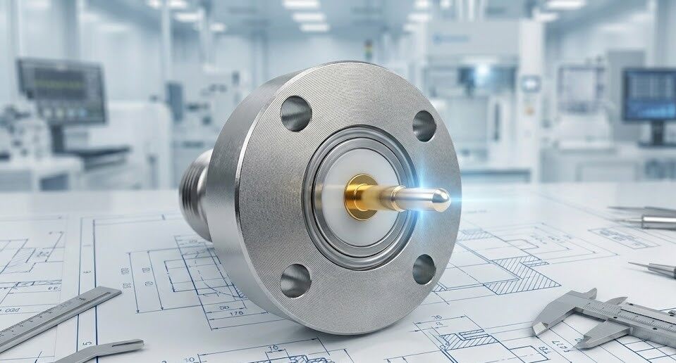
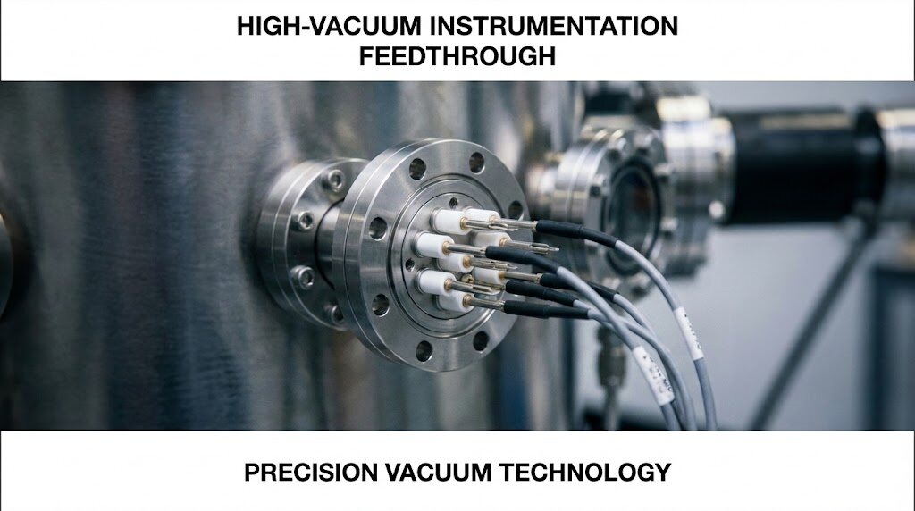
Regardless of whether one chooses RF plasma or MW plasma, the energy must be coupled into a vacuum chamber. This requires a "window" or a "cavity"—a physical barrier that holds the vacuum but lets the electromagnetic energy pass through. This component, often a dielectric tube, bell jar, or plate, is the "generation site" of the plasma.
Selecting the material for this cavity is one of the most critical engineering decisions in plasma system design. It faces a brutal trinity of challenges:
The three primary contenders are Quartz (SiO2), Alumina (Al2O3), and Yttrium Oxide (Y2O3, commonly called Yttria). While Quartz and Alumina have been industry standards, Yttria is emerging as the critical enabler for next-generation processes.
Fused silica (Quartz) is the most common material for general-purpose plasma tubes.
The reaction product, Silicon Tetrafluoride, is a gas. This means the Quartz wall literally evaporates. This leads to rapid wall thinning, frequent replacement, and the release of oxygen contaminants that can ruin the process chemistry.
Alumina is mechanically stronger and more chemically resistant than Quartz.
For high-end MW plasma and RF plasma applications—specifically those involving corrosive etchants or requiring ultra-high purity (like diamond growth)—Yttrium Oxide (Yttria) is the recommended material.
The primary reason to recommend Yttria is its unique thermodynamic interaction with halogen plasmas.
Passivation: When Yttria is exposed to Fluorine plasma, it reacts to form Yttrium Fluoride (YF3).
Crucially, YF3 is a stable, non-volatile solid with a very high melting point. It creates a "passivation layer" on the surface of the ceramic. Once this thin layer forms, it acts as a shield, preventing the plasma from eating further into the ceramic.
Erosion Rate: Comparative studies show that the erosion rate of Yttria in high-density CF4 plasma is nearly zero, whereas Quartz erodes rapidly. Data suggests Yttria can last 10 to 100 times longer than Quartz or Alumina in these aggressive environments.
Implementing a Yttriacavity presents engineering challenges due to cost and brittleness. Consequently, two main approaches are used:
| Plasma Environment | Recommended Material | Reasoning |
|---|---|---|
| Non-Corrosive (Ar, O2, N2) | Quartz | Economical, excellent thermal shock resistance, lowest dielectric loss. |
| Moderate Corrosive / High Heat | Alumina | Mechanically robust, better chemical resistance than quartz, but risks particle contamination. |
| Halogen Etching (F, Cl) | Yttria (Y2O3) | Strongly Recommended. Forms protective YF3 layer. Lowest erosion rate. No particulate contamination. |
| Diamond Growth (MPCVD) | Solid Yttria | Prevents Silicon contamination (from quartz) which degrades diamond quality. Withstands high thermal load if cooled correctly. |
The distinction between radio frequency plasma and microwave plasma is a tale of two frequencies. RF plasma (13.56 MHz) is the force of kinetic precision, leveraging ion inertia to create the high-voltage sheaths necessary for sculpting the microscopic architecture of modern electronics. Microwave plasma (2.45 GHz) is the force of chemical abundance, leveraging electron resonance to generate the dense, reactive environments required for synthesizing new materials like diamond and abating industrial waste.
Yet, the power of these plasmas is only as good as the vessel that contains them. As industrial demands for purity and durability rise, the traditional reliance on Quartz and Alumina is faltering. Yttrium Oxide (Yttria) has emerged as the superior choice for the generation cavity. Its ability to forge a self-protective shield against corrosive plasmas makes it the indispensable armor of the plasma processing industry. For any engineer designing the next generation of MW or RF plasma systems, the adoption of Yttria-based ceramics is not just an upgrade; it is a necessity for survival in the harsh environment of the fourth state of matter.
? - scientific articles - news - CERAMIC-SOLUTIONS")
? - scientific articles - news - CERAMIC-SOLUTIONS")