Power Feedthrough Technology Report
Introduction
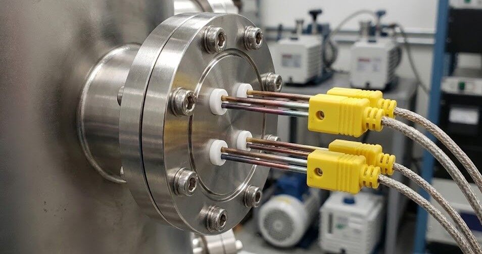
The transmission of electrical energy across a pressure boundary represents one of the most persistent challenges in vacuum science and high-pressure engineering. Power feedthroughs serve as the critical interface, enabling the transfer of electrical currents—ranging from picoampere instrumentation signals to kilovolt, multi-kilowatt power loads—into hermetically sealed environments. These components are foundational to the operation of semiconductor manufacturing equipment, particle accelerators, nuclear fusion reactors, and aerospace systems. The engineering of a power feedthrough is a multidisciplinary exercise requiring the reconciliation of contradictory requirements: the device must be an electrical conductor yet a vacuum seal; it must dissipate massive thermal loads yet withstand the mechanical stresses of disparate thermal expansion coefficients; and it must resist dielectric breakdown in environments where the physics of electrical discharge differs radically from atmospheric conditions.
This report provides an exhaustive technical analysis of power feedthrough technology. It delineates the fundamental physics of vacuum electrical breakdown, contrasts the microstructural and thermal properties of advanced ceramic insulators (Alumina, Aluminum Nitride, Silicon Nitride), and examines the metallurgical joining processes that ensure hermeticity. Furthermore, it details specific application requirements in plasma etching and nuclear fusion, providing rigorous data on failure modes and design margins.
Fundamental Physics of Operation
The operational integrity of a power feedthrough is defined by its ability to maintain a vacuum-tight seal (typically < 1 × 10⁻⁹ mbar·L/s for Ultra-High Vacuum applications) while preventing electrical arcing. This functionality is governed by two distinct physical regimes: the air-side (atmospheric pressure) and the vacuum-side (low pressure), separated by the dielectric feedthrough body.
Electrical Breakdown Mechanisms and Paschen’s Law
The transition from atmospheric pressure to vacuum fundamentally alters the insulation capability of the gas medium surrounding the conductor. This non-linear behavior is described by Paschen’s Law, which establishes that the breakdown voltage (Vb) of a gas is not a constant but a function of the product of gas pressure (p) and the distance between electrodes (d).
The governing equation is derived from the Townsend avalanche mechanism:
Vb = (B · pd) / [ ln(A · pd) - ln(ln(1 + 1/γse)) ]
Where A and B are gas-specific constants related to the saturation ionization and excitation energies, and γse is the secondary electron emission coefficient of the cathode material.

The Paschen curves for air, argon, and helium highlight the regions with the lowest breakdown voltages. This nonlinear relationship indicates that gases are particularly prone to arcing under specific combinations of pressure and distance.
The Paschen Minimum Application
As pressure decreases from atmospheric levels (760 Torr) towards the rough vacuum regime, the mean free path of electrons increases. This allows electrons to accelerate to higher kinetic energies between collisions with neutral gas molecules. However, as pressure continues to drop, the density of gas molecules decreases to the point where the probability of an ionizing collision diminishes. Consequently, the breakdown voltage drops to a minimum value—the Paschen minimum—before rising steeply in the high vacuum regime.
|
Gas Type
|
Minimum Breakdown Voltage
|
Product of Pressure and Distance at Vmin
|
Breakdown Field Strength (at 1 atm, 0.75 cm gap)
|
|
Air
|
~327 V
|
0.57 Torr·cm
|
~30 kV/cm
|
|
Ar
|
~137 V
|
0.9 - 1.2 Torr·cm
|
~7 kV/cm
|
|
He
|
~156 V
|
4.0 Torr·cm
|
~1-2 kV/cm
|
|
SF6
|
~500+ V
|
(Varies)
|
~89 kV/cm
|
Engineering Implication:
Power feedthroughs operating in the "Paschen minimum" regime are critically vulnerable to arcing. This pressure range is ubiquitous in semiconductor plasma processing chambers. To mitigate this, feedthroughs are designed with specific geometries to artificially increase the path length or eliminate the gas gap entirely through potting. A standard design solution involves a "labyrinth" shield or a convoluted ceramic geometry that forces any discharge path to traverse a distance significantly larger than the mean free path, thereby pushing the effective pd value to the right of the Paschen curve minimum.
High Vacuum Breakdown and Surface Flashover
In high vacuum environments (< 10-5 Torr), the mean free path of an electron exceeds the gap distance between conductors. In this regime, gas ionization is no longer the primary breakdown mechanism. Instead, failure occurs via surface phenomena.
-
Field Emission: At high electric field strengths (> 107 V/m), electrons are stripped from the metal lattice of the conductor at microscopic irregularities via quantum tunneling. This current can heat local spots on the anode, releasing adsorbed gas which is then ionized, initiating a breakdown arc.
-
Surface Tracking: Electrons traverse the surface of the ceramic insulator rather than the vacuum gap. This mechanism is heavily influenced by the Secondary Electron Emission Yield of the ceramic material. If the SEEY coefficient is greater than 1, a single impacting electron releases multiple secondary electrons. This leads to a multipactor effect—a resonant electron avalanche that charges the ceramic surface positively, distorting the local electric field and inducing a flashover across the insulator surface. Advanced feedthroughs for high-voltage applications often employ surface coatings (such as Titanium Nitride or Chrome Oxide) to suppress SEEY.
Thermal Transport and Joule Heating
Feedthroughs carrying high currents generate significant resistive heat (Q = I2R). Unlike in atmospheric conditions, where convective air cooling aids heat dissipation, vacuum-side conductors rely almost exclusively on conduction through the ceramic insulator and radiation.
The thermal resistance network of a feedthrough is complex. The heat must pass from the central conductor, across the conductor-ceramic interface, through the bulk ceramic, across the ceramic-flange interface, and finally to the chamber wall. The most significant thermal bottleneck is often the ceramic insulator itself. The resulting ΔT generates mechanical stress due to the Coefficient of Thermal Expansion mismatch between the metal conductor and the ceramic.
σthermal = (E · α · ΔT) / (1 - ν)
Where E is Young's modulus, α is the CTE, and ν is Poisson's ratio. If σthermal exceeds the flexural strength of the ceramic or the shear strength of the braze joint, the hermetic seal will fail catastrophically.
Ceramic Insulator Materials: Comparative Microstructure and Performance
The choice of insulator material dictates the feedthrough's voltage rating, thermal capacity, and mechanical robustness. While Al2O3 remains the industry standard, high-performance applications increasingly utilize AlN and Si3N4 for their superior thermal and mechanical properties.
Al2O3: The Industry Standard
Alumina is categorized by its purity, which fundamentally defines its processing and performance.
94% - 96% Alumina:
-
Microstructure: This grade contains 4-6% sintering aids, typically SiO2, MgO, CaO. During sintering, these impurities form a glassy grain boundary phase.
-
Role in Sealing: This glassy phase is crucial for the Mo-Mn metallization process (detailed in Section 4). The glass migrates into the metallization layer, creating a mechanical interlock.
-
Performance: It offers moderate thermal conductivity (~20-25 W/mK) and good dielectric strength. However, the glassy phase increases the dielectric loss tan δ, causing self-heating under RF loads.
99% - 99.8% Alumina:
-
Microstructure: High purity with minimal glassy phase.
-
Performance: Exhibits higher mechanical hardness, superior dielectric strength (>17 kV/mm), and a significantly lower dielectric loss tangent. This makes it essential for RF applications where dielectric heating must be minimized.
-
Processing Challenge: The lack of a glassy phase renders standard Mo-Mn metallization ineffective. Joining requires AMB or exotic thin-film metallization.
AlN: The Thermal Management Solution
Aluminum Nitride is a covalently bonded non-oxide ceramic valued for its exceptional thermal conductivity.
-
Thermal Conductivity: AlN offers thermal conductivity in the range of 170 - 220 W/mK, which is 7-10 times higher than Alumina and approaching that of metallic Aluminum. The mechanism of heat transfer is phonon transport; consequently, oxygen impurities in the lattice severely degrade this property, necessitating high-purity processing.
-
CTE Matching: Its CTE (~4.5 × 10⁻⁶/°C) is a very close match to Silicon (~2.6 - 3 × 10⁻⁶/°C) and Molybdenum. This property is critical in semiconductor applications to minimize thermal stress on silicon wafers or Mo electrodes.
-
Drawbacks: AlN is difficult to metallize and oxidizes above 700°C in air, forming an alumina surface layer that can inhibit heat transfer.
Si3N4: Mechanical Superiority
Silicon Nitride is chosen for its extreme mechanical toughness.
-
Fracture Toughness: Si3N4 has a fracture toughness (KIC) of 5-7 MPa·m1/2, compared to 3-4 for Alumina. This makes it highly resistant to crack propagation and catastrophic failure under mechanical shock.
-
Thermal Shock Resistance: Its low CTE (~3.0 × 10⁻⁶/°C) combined with high strength allows it to withstand rapid temperature changes that would fracture Alumina.
-
Application: Used in highly stressed structural feedthroughs and aerospace components where reliability is paramount.
Detailed Material Properties Comparison
Table 2: Comparative Properties of Ceramic Insulators for Feedthroughs
|
Property
|
Unit
|
96% Al2O3
|
99% Al2O3
|
AlN
|
Si3N4
|
|
Thermal Conductivity
|
W/m·K
|
24 - 28
|
30 - 35
|
170 - 220
|
20 - 30
|
|
CTE (25-400°C)
|
10-6/°C
|
7.1
|
7.2
|
4.6 (Matches Si)
|
3.0
|
|
Dielectric Strength
|
kV/mm
|
10 - 15
|
17 - 25
|
15 - 20
|
15
|
|
Flexural Strength
|
MPa
|
350
|
380
|
300 - 350
|
800 - 900
|
|
Dielectric Constant @ 1 MHz
|
-
|
9.0
|
9.8
|
8.8
|
8.0
|
|
Dissipation Factor (tan δ)
|
-
|
3 × 10⁻⁴
|
1 × 10⁻⁴
|
5 × 10⁻⁴
|
10 × 10-4
|
|
Primary Metallization
|
-
|
Mo-Mn
|
AMB / Thin Film
|
AMB
|
AMB
|
Hermetic Sealing and Joining Technologies
The core technology of a feedthrough is the CTM seal. This joint must remain hermetic under thermal shock (cryogenic to >450°C), mechanical vibration, and pressure cycling. Two primary technologies dominate the industry: Molybdenum-Manganese Metallization and Active Metal Brazing.
Mo-Mn Metallization Process
This is the traditional and most mature method for joining 94-96% alumina to metals. It relies on a multi-step chemical reaction to create a wettable surface on the ceramic.
Step-by-Step Process Mechanism:
-
Slurry Application: A paint-like slurry containing Mo and Mn powders, along with binders, is screen-printed or brushed onto the ceramic surface.
-
Sintering: The coated ceramic is fired in a wet hydrogen atmosphere (dew point controlled to ~25°C) at approximately 1400°C.
-
Reaction 1: The moisture in the hydrogen oxidizes the Manganese to MnO.
-
Reaction 2: The MnO reacts with the SiO2 glass phase inherent in the alumina ceramic to form a low-melting-point manganese silicate glass.
-
Migration: This low-viscosity glass migrates from the bulk ceramic into the porous Molybdenum layer, locking the metal particles to the ceramic surface upon cooling.
-
Plating: The resulting sintered Mo-Mn layer is conductive but difficult to braze. It is typically electroplated or electroless-plated with Ni to enhance wettability.
-
Brazing: The metallized ceramic is brazed to a metal flange (typically Kovar) using a Silver-Copper eutectic alloy (BAg-8, 72% Ag / 28% Cu).
Advantages: Extremely high bond strength (often exceeding the tensile strength of the ceramic itself, >200 MPa), high hermetic reliability.

A schematic cross-sectional view of the Mo-Mn metallization layer on alumina ceramic. The figure illustrates how the glassy phase migrates from the ceramic bulk to the porous molybdenum layer, thereby achieving mechanical interlocking.
Limitations: Cannot be used effectively on high-purity (99%+) alumina or non-oxide ceramics due to the absence of the necessary glassy silicate phase.
AMB
AMB represents a significant advancement, eliminating the pre-metallization step and allowing direct joining of metal to almost any ceramic.
Process Mechanism:
-
AMB utilizes braze alloys doped with "active" elements—typically Ti, Zr, or V.
-
Assembly: The ceramic and metal components are assembled with the AMB foil or paste (e.g., Ag-Cu-Ti) in between.
-
Vacuum Brazing: The assembly is heated in a high vacuum furnace (< 10-5 Torr).
-
Active Reaction: As the braze melts (~800-900°C), the Titanium migrates to the ceramic interface.
-
Chemistry: The Ti reacts with the ceramic surface to form a reaction layer. For Alumina, it forms TiOx; for AlN, it forms TiN.
-
Wetting: The bulk Silver-Copper alloy wets this newly formed reaction layer, creating a hermetic seal.
Advantages: Single-step process; enables joining of high-performance ceramics (AlN, SiC, Si3N4) and high-purity alumina.
Limitations: The reaction layer can be brittle; the process requires rigorous vacuum control to prevent oxidation of the active titanium before it can react with the ceramic. Tensile strength is generally lower than Mo-Mn seals (approx. 70-100 MPa vs 200+ MPa).
CTE Matching
A critical failure mode in CTM seals is residual stress generated during the cooling phase of the brazing process. If the metal contracts significantly more than the ceramic, it can induce compressive stress that crushes the ceramic or tensile stress that delaminates the joint.
Material Selection for CTE Matching:
-
Kovar (ASTM F15): An Iron-Nickel-Cobalt alloy specifically engineered to have a non-linear CTE curve that closely tracks Borosilicate glass and Alumina (~5.5 × 10⁻⁶/°C up to 400°C). It is the standard material for weld collars and sleeves.
-
Stainless Steel 304: Has a high CTE (~17 × 10-6/°C). Direct brazing of Stainless Steel to Alumina in a concentric geometry usually results in cracking.
-
Stress-Relief Design: To utilize stainless steel flanges, a "sandwich" or "stress-relief" design is employed. A thin Kovar sleeve is brazed to the ceramic, and the flexible Kovar sleeve is then TIG welded to the rigid Stainless Steel flange. This decouples the thermal mismatch.
Design Engineering: Geometry and Standards
Creepage and Clearance Optimization
To prevent arcing on the air-side (atmospheric side) of the feedthrough, the insulator geometry must be carefully optimized.
-
Creepage Distance: The shortest distance along the surface of the solid insulating material between two conductive parts. Surface contamination (dust, moisture) can create a conductive path, leading to tracking failure. To mitigate this, insulators are designed with "ribs," "skirts," or convolutions. These features significantly increase the surface path length without increasing the overall height of the component.
-
Clearance: The shortest distance through the air between two conductive parts.

A schematic diagram of creepage distance and clearance on a high-voltage insulator. The corrugated design ("skirt") significantly increases the creepage distance along the surface (red dashed line), while having little effect on the straight air gap (blue dashed line).
Pollution Degrees (IEC 60664-1):
-
Degree 1: No pollution or only dry, non-conductive pollution (e.g., clean room).
-
Degree 2: Only non-conductive pollution occurs, except for occasional temporary conductivity caused by condensation (e.g., laboratory).
-
Degree 3: Conductive pollution occurs, or dry non-conductive pollution becomes conductive due to condensation (e.g., industrial factory).
Design Rule: For a 1000V operating voltage in Pollution Degree 2, a minimum creepage of ~5-10 mm is required. However, for high-reliability vacuum feedthroughs, safety factors of 2.0x to 3.0x over IEC standards are common practices.
Conductor Configurations
The choice of conductor material represents a trade-off between electrical conductivity, thermal properties, and mechanical strength.
-
OFHC Copper: The standard for high current applications (100A - 1000A). It has the highest electrical and thermal conductivity but is soft and mechanically weak. Copper pins are typically brazed into a Kovar cap to provide a robust sealing surface.
-
Molybdenum: Used for high stiffness and high-temperature tolerance. Its conductivity is lower than copper (approx. 30% IACS), but its CTE matches ceramics well, allowing for larger diameter pins without excessive thermal stress.
-
Nickel: Selected for its excellent corrosion resistance, particularly in semiconductor etch environments involving halogens. It is ferromagnetic, which may be undesirable in electron microscopy applications.
Application Case Studies
Semiconductor Manufacturing: Plasma Etch and PVD
Modern semiconductor fabrication relies on processes like RIE and PECVD.
-
RF Power Transmission: Feedthroughs must transmit high-frequency energy (13.56 MHz, 60 MHz, or even microwave frequencies). At these frequencies, the "skin effect" forces current to flow only on the surface of the conductor, increasing resistive heating. Furthermore, dielectric heating within the ceramic becomes significant (Ploss ∝ f · V2 · tan δ). High-purity 99.8% Alumina or AlN is required to minimize the loss tangent and prevent thermal runaway.
-
Corrosive Resistance: Process gases often contain highly reactive Fluorine (SF6, CF4) or Chlorine radicals. Standard Silver-Copper braze alloys are rapidly corroded by these species. Solutions include using Gold-based braze alloys (Au-Ni) or applying protective ceramic coatings over the braze joint.
-
Thermal Management: As wafer bias powers exceed 10 kW, the heat load on the feedthrough becomes critical. AlN feedthroughs are standard in high-power Electrostatic Chucks (ESCs) to conduct heat away from the RF rod to the water-cooled baseplate.
Nuclear Fusion (ITER and Tokamaks)
Feedthroughs in fusion reactors face arguably the most hostile environment in modern engineering.
-
Neutron Radiation Damage: High-energy neutrons (14 MeV from D-T fusion) bombard the feedthrough components.
-
Displacement Damage: Neutrons displace atoms in the crystal lattice, causing "swelling" in ceramics. Differential swelling between the ceramic and the metal components can fracture the seal.
-
Electrical Degradation: RIC causes the ceramic to become momentarily conductive during pulses. Long-term RIEBS reduction permanently degrades insulation capability.
-
Tritium Containment: Feedthroughs serve as the primary vacuum boundary for the torus vessel, which contains radioactive Tritium fuel. They must meet SIC standards. Designs often feature double-barriers with an actively pumped interspace to detect and capture any leakage before it reaches the atmosphere.
-
Remote Handling: Due to activation, feedthroughs must be designed for installation and removal by robotic manipulators, requiring specialized "quick-connect" features that are robust against galling.
Aerospace and Satellite Systems
-
Multipactor Discharge: In the vacuum of space, RF components are susceptible to multipactor discharge—a resonant condition where electrons bounce back and forth between electrode surfaces in sync with the RF field, liberating more electrons with each impact. This can destroy the device.
-
Thermal Cycling: Satellites in Low Earth Orbit (LEO) experience a thermal cycle every 90 minutes, swinging from -100°C (eclipse) to +150°C (sunlight). The low-cycle fatigue life of the ceramic-to-metal braze joint is the primary life-limiting factor for these components.
Reliability and Failure Analysis
Leakage Mechanisms and Testing
The "hermeticity" of a feedthrough is verified using Helium Mass Spectrometry.
-
Standard: A typical pass/fail criterion is a leak rate of < 1 × 10⁻⁹ mbar·L/s.
-
Virtual Leaks: A common failure in design is the "virtual leak"—a trapped volume of gas within the feedthrough assembly (e.g., at the bottom of a blind threaded hole or between concentric tubes) that slowly outgasses into the vacuum, mimicking a real leak. All internal cavities must be vented.
-
Permeation: While metals and ceramics are effectively impermeable to gases, helium can permeate through glass and certain elastomers over long periods. However, for ceramic-to-metal seals, permeation is negligible compared to potential leak paths at the braze interface.
Mechanical Failure Modes
-
Interface Delamination: Occurs when shear stresses exceed the bond strength. In Mo-Mn seals, this often manifests as the plating peeling off the ceramic. In AMB seals, the failure typically occurs within the brittle reaction layer.
-
Ceramic Cracking: Often caused by overtightening the air-side connection. If a heavy cable places a bending moment on the conductor, the rigid ceramic can fracture. "Floating" conductor designs allow the pin to move slightly, decoupling external mechanical loads from the vacuum seal.
Conclusion
The engineering of power feedthroughs is a convergence of advanced materials science, vacuum physics, and precision manufacturing. While 96% Alumina coupled with Mo-Mn metallization remains the robust, cost-effective standard for general vacuum applications, the technological frontier is shifting. AlN joined via AMB is becoming the baseline for high-performance sectors, driven by the intense thermal management requirements of semiconductor processing and the radiation hardness needs of fusion energy. Future developments are focused on "smart" feedthroughs with integrated fiber-optic sensors for real-time monitoring of temperature and strain, as well as FGMs that eliminate the sharp interface between metal and ceramic, theoretically removing the CTE mismatch limitation entirely.