28-February-2026
With the development of 3D advanced packaging (such as TSV, HBM, 3D NAND), semiconductor manufacturing often requires wafers to be accurately thinned down to 50 micrometers or even below 10 micrometers. As the thickness enters the micrometer scale, the rigidity of the wafer significantly declines, making it much more vulnerable to damage during processing. Traditional metal vacuum chucks with holes, due to localized negative pressure concentration, easily cause localized stress concentration and microscopic collapse (dimples) on ultrathin wafers at the hole locations, which affects the Total Thickness Variation (TTV) metrics and increases the risk of wafer cracking. Porous ceramic chucks, featuring a uniformly distributed microscopic pore network, can provide a relatively uniform negative pressure distribution, thereby effectively mitigating localized stress concentration. This is currently a common technical approach to solving the deformation and micro-cracking issues in ultrathin wafer thinning processes.
In manufacturing scenarios such as 3D chip stacking, MEMS, and high-voltage power devices, the physical thickness of the wafer directly affects the parasitic parameters of electrical interconnections and the heat dissipation efficiency of the devices. The process of transforming a macroscopic-thickness silicon ingot slice into a flexible thin film mainly relies on Mechanical Grinding and Chemical Mechanical Planarization (CMP).
Mechanical grinding is usually divided into two stages: coarse grinding and fine grinding. In the coarse grinding stage, the silicon substrate is rapidly removed using a relatively coarse-grit (e.g., 400-grit) diamond grinding wheel at a high spindle speed, but this leaves mechanical damage and residual stress on the sub-surface. The fine grinding stage switches to a finer grinding wheel (1200-grit and above) to refine the surface topography and approach the target thickness. Finally, the damage layer is typically gently removed and stress is relieved using CMP or dry polishing technologies.
Throughout this series of processing steps, the wafer must continuously withstand the Z-axis downward shear force and horizontal rotational friction force from the grinding wheel above. Due to the extremely weak rigidity of the wafer resulting from the reduced thickness, if the bottom clamping system (chuck) has micrometer-level uneven support forces or surface undulations, it can cause the wafer to deform or crack when subjected to stress.
Traditional metal chuck surfaces are usually machined with concentric grooves or discrete macroscopic vacuum suction holes (diameters typically ranging from hundreds of micrometers to millimeters). When handling ultrathin wafers, this discontinuous physical topological structure is prone to the following process issues:
When the system establishes vacuum negative pressure, the ultrathin wafer suspended directly above the vacuum holes or grooves will experience a slight downward deflection (Dimple) under the pressure differential. During the dynamic grinding process, the rigid grinding wheel above will unselectively grind and flatten these forced-deflection areas along with the surrounding flat areas. After processing is complete and the vacuum is released, the wafer undergoes elastic rebound due to the release of internal stress, and the previously deflected areas will bulge upward, resulting in shallow pit marks on the backside of the wafer corresponding to the chuck holes. This microscopic thickness variation directly affects the TTV (Total Thickness Variation) metrics, adversely impacting subsequent hybrid bonding or high-precision lithography processes that require high coplanarity.
Ultrathin wafers (especially compound semiconductor materials with high brittleness such as SiC and GaN) are highly sensitive to nonlinear deformation. At the edges of the metal chuck holes, geometric discontinuities can easily trigger high tensile stress. Under the tearing action of the localized high-stress field, native sub-micron defects or scratches on the wafer surface can easily initiate sharp micro-cracks. During subsequent forceful CMP friction, thermal cycling, or mechanical debonding from the chuck, these latent micro-cracks are highly prone to propagation, thereby increasing the risk of overall wafer shattering.
Through classical elasticity theory, the impact of the chuck surface topology on the deformation of ultrathin wafers can be quantitatively evaluated. Based on Kirchhoff's thin plate bending theory, the core functional relationship between the maximum deflection (depth of downward deformation) wmax of the wafer at the center of the vacuum hole and the process parameters can be approximately expressed as:
(where P is the pressure differential between the internal negative pressure of the hole and the external atmospheric pressure, r is the effective radius of the suction hole, and t is the wafer thickness).
This formula reveals a key mechanical characteristic in the thinning process: the local ultimate deformation depth of the wafer is inversely proportional to the cube of the wafer thickness. When the wafer thickness t is thinned from 500 micrometers to 50 micrometers (i.e., reduced to 1/10), its local flexural rigidity drops to one-thousandth of its initial state. If the macroscopic suction hole radius r of the traditional chuck remains unchanged, the local deflection depth will increase significantly. Therefore, to engineer the global TTV deviation to an extremely low level (such as below 0.5 micrometers), a more feasible physical path is to substantially reduce the effective radius r of the vacuum holes and construct a continuous and uniform negative pressure distribution field on the contact surface.
To address the operational difficulties of ultrathin wafers being extremely prone to breakage and curling, the industry has developed specialized backside thinning processes such as TAIKO. This process uses a dedicated grinding wheel with a protective ring profile, intentionally leaving an original-thickness edge ring of about 3 mm in width at the outermost periphery of the wafer during grinding, and only performing deep thinning on the inner core area.
The thick edge ring retained at the periphery acts as a physical load-bearing framework, significantly enhancing the planar bending mechanical strength of the overall thin-film wafer, reducing the risk of curling in subsequent handling, and effectively avoiding the edge chipping issues common in standard full-surface thinning.
However, this also imposes higher requirements on the underlying chuck. The extremely thin central area almost completely loses its rigidity during grinding, and there is an edge step drop of hundreds of micrometers. At this point, any minute pressure gradient unevenness or support surface undulation from the back of the chuck can easily be amplified by the thin-film area and converted into TTV errors. Therefore, the TAIKO process usually needs to be used in conjunction with a support system offering superior surface uniformity.
Porous Ceramic chucks are made of nano- or sub-micron ceramic powders through a sintering process, creating a vast network of interconnected microscopic pores internally. This structure alters the transmission method of vacuum negative pressure, providing more uniform support for ultrathin wafer processing.
Compared to the millimeter-scale macroscopic holes of traditional metal chucks, porous ceramics usually control the effective suction hole diameter to range from 1-2 micrometers to tens of micrometers. According to the formula wmax ∝ (P · r4) / t3, the significant reduction in the effective radius r of the suction contact points can drastically reduce the deformation depth of the wafer under local stress in the theoretical model. The fluid damping generated by the micro-pore network allows the negative pressure to permeate uniformly across the entire ceramic contact surface, mitigating stress concentration to a certain extent, thereby helping to alleviate the Dimple effect and maintain good TTV metrics.
In current manufacturing systems, based on comprehensive considerations of cost, thermodynamic response, and mechanical strength, porous ceramics are mainly divided into two material systems: alumina and silicon carbide:
| Key Physical Properties | Porous Alumina (Al2O3) | Porous Silicon Carbide (SiC) |
|---|---|---|
| Apparent Density (g/cm³) | 2.3 - 2.5 | 2.0 - 2.2 |
| Sintered Pore Size Range (μm) | 1 ~ 100 (Wider adjustable range) | 15 ~ 50 |
| Coefficient of Thermal Expansion (×10-6/K) | 7.4 | 4.7 (Close to single-crystal silicon) |
| Thermal Conductivity | Standard | Superior |
Widely used with mature sintering technology, it can precisely control the pore size distribution to 2-5 micrometers. This fine pore size provides more meticulous support and is a common choice for standard wafer thinning and process scenarios with high requirements for local deformation (Dimple) control.
Possesses excellent lattice thermal conductivity, and its thermal expansion coefficient matches that of single-crystal silicon more closely. In heavy-load coarse grinding processes for high-hardness materials like silicon carbide and sapphire, a large amount of frictional heat is generated. Porous SiC chucks can quickly conduct and dissipate heat in coordination with the underlying cooling system, helping to reduce wafer expansion and warpage caused by thermal stress, thereby maintaining better thermal TTV control.
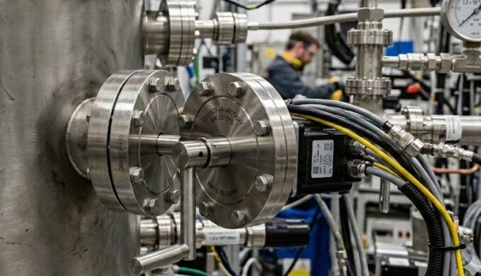
To meet high-precision mass production requirements, mainstream semiconductor thinning and dicing equipment manufacturers in the industry (such as DISCO, OKAMOTO, etc.) generally equip their high-end models with porous ceramic chucks as an important configuration.
For example, the fully automatic grinder/polisher introduced by DISCO (e.g., model DGP8761) widely incorporates porous ceramic chucks in its Z1 and Z2 axis high-speed grinding, as well as the Z3 axis stress-relief polishing stages. The dynamic global thickness feedback correction mechanism (Auto-TTV) equipped on this model has high requirements for the physical stability of the underlying clamping surface. The uniform physical reference provided by the porous ceramic chuck helps reduce measurement interference caused by local material yielding, allowing the thickness compensation algorithm to operate smoothly.
On the other hand, OKAMOTO's ultra-precision surface grinders, when processing large-sized hard wafers, often use a composite chuck structure combining a structural ceramic skeleton with a highly thermally conductive silicon carbide filler. Paired with its highly rigid bed and micro-feed servo system, precision machining controls the macroscopic contour roughness and overall flatness error of the porous ceramic surface within strict tolerance zones (often at the sub-micron level), thereby ensuring the long-term stability and machining accuracy of the processing equipment.
As advanced semiconductor processes evolve toward 3D heterogeneous stacking, the significant reduction in wafer thickness has made mechanical vulnerability during processing an engineering challenge that cannot be ignored. Traditional macroscopic-hole vacuum solid chucks are prone to causing localized stress concentration when handling ultrathin wafers, leading to surface deformation (Dimples) and the expansion of micro-cracks. Relying on an interconnected microscopic pore network, porous ceramic chucks alter the form of vacuum negative pressure application, achieving relatively uniform adsorption and support. Combined with optimizations in pore size and materials (such as alumina and silicon carbide), and paired with high-precision processing equipment, this technical approach can effectively reduce the breakage rate in ultrathin wafer processing and improve TTV accuracy. It is currently an important foundational support solution in the advanced manufacturing process chain.