Technical Article
OLED Mura Defects in Manufacturing: Causes and Vacuum Chuck Solutions
OLED Mura defects are localized variations in brightness, color, or texture across a display. In manufacturing, they can originate from three interacting cause families: electrical non-uniformity in the backplane, variation in deposited or printed films, and mechanical distortion during substrate handling. A vacuum chuck becomes a credible root cause when the Mura pattern follows the chuck geometry, changes with vacuum settings, or correlates with measured substrate dimpling. The right response is therefore not to replace every chuck, but to connect the optical signature to physical and process evidence.
What Is an OLED Mura Defect?
Mura is a general display-industry term for visible non-uniformity. It can appear as cloudy regions, spots, lines, bands, color shifts, or a repeated grid. The same visual symptom can have different physical causes, which is why “Mura” should be treated as a defect class rather than a single failure mechanism.
In an OLED panel, emitted luminance depends on the electrical drive delivered by the thin-film transistor backplane and on the optical and electrical behavior of the deposited device stack. Local differences in transistor characteristics, organic-layer thickness, electrode condition, encapsulation stress, or surface topography can therefore produce similar visible patterns. Reviews of display-Mura inspection also distinguish multiple shapes and detection approaches rather than assigning every non-uniformity to one source.
The manufacturing question is not simply “Is there Mura?” It is “Which process variable creates a spatial signature that matches the observed Mura?”
Article Navigation
- Three main OLED Mura manufacturing causes
- How vacuum chuck dimpling can become OLED Mura
- Why porous ceramic changes load distribution
- How to determine whether the chuck is the root cause
- How to select and qualify a porous ceramic chuck
Three Main OLED Mura Manufacturing Causes
1. Electrical and Backplane Variation
Active-matrix OLED pixels are driven by thin-film transistor circuits. Variations in threshold voltage, mobility, leakage, contact resistance, or supply distribution can change pixel current and produce luminance non-uniformity. Compensation circuits and calibration algorithms are designed specifically because transistor characteristics are not perfectly identical across a large panel, as recent LTPO pixel-circuit research illustrates.
Electrical Mura often changes with gray level, refresh condition, temperature, or drive history. If the defect follows circuit rows, columns, or backplane regions but does not correlate with substrate topography, the investigation should start with electrical measurements rather than the vacuum fixture.
2. Film Formation and Process Variation
OLED performance also depends on uniform functional layers. Printing, coating, evaporation, drying, and curing conditions can alter local film profiles. Research on inkjet-printed OLEDs, for example, shows that ink properties and vacuum-drying conditions influence the final film shape. Similar reasoning applies to other process steps: a non-uniform wet film, deposition shadow, contamination event, or thermal gradient can become an optical non-uniformity after the device is completed.
Film-related Mura may follow nozzle paths, coating directions, mask features, chamber flow, or thermal zones. These signatures should be compared with equipment history and in-line metrology before mechanical handling is blamed.
3. Mechanical Handling and Substrate Topography
Flexible OLED manufacturing introduces a third risk: a thin polymer substrate or temporarily bonded flexible stack must be held flat while it passes through precision processes. Local pressure gradients, unsupported spans, particles, grooves, or discrete vacuum holes can create temporary or residual topography. Electromechanical studies of thin films on polymer substrates also show why strain, cracking, and electrical behavior must be considered together rather than as separate disciplines.
If coating, printing, lamination, exposure, or inspection occurs while the substrate is distorted, the topography can affect local process conditions. A depression may change a coating gap, alter wet-film redistribution, disturb focus, or concentrate stress. The eventual optical defect can then preserve the spatial pattern of the handling surface.
This mechanical path is most plausible when the defect repeats at the pitch of vacuum holes or grooves, changes after chuck cleaning or vacuum adjustment, or appears after a specific handling step.
How Vacuum Chuck Dimpling Can Become OLED Mura
The causal chain should be tested step by step:
- A pressure difference is applied across a thin substrate.
- A portion of the substrate spans a hole, groove, recess, or poorly supported area.
- The unsupported region deflects under pressure.
- A downstream process occurs while the substrate is not locally planar.
- The process creates a thickness, focus, stress, or contact variation.
- The variation changes pixel current, optical interference, emission efficiency, or encapsulation integrity.
- The completed panel shows a spatially correlated Mura pattern.
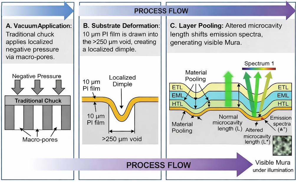
Skipping any link in this chain can lead to a false diagnosis. A visible grid alone is suggestive, but it is not proof. The team should compare the grid pitch and orientation with the fixture, repeat the process at different vacuum levels, and measure the substrate or a witness film directly.
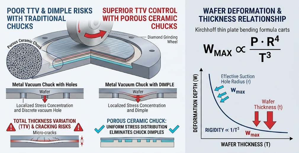
A Useful Thin-Plate Screening Relationship
For a small-deflection plate model, the center deflection scales approximately as:
w ∝ Δp · a4 / (E · t3)
Here, w is deflection, Δp is pressure difference, a is the unsupported span, E is elastic modulus, and t is substrate thickness.
This relationship is a screening tool, not a universal design equation. Real polymer films can have residual stress, anisotropy, multilayer construction, imperfect boundary conditions, and large-deflection membrane behavior. Even so, the scaling is valuable: unsupported span has a fourth-power influence in the simple plate regime, while thickness enters with a third-power influence. Reducing the effective span can therefore be more powerful than making a modest vacuum adjustment.
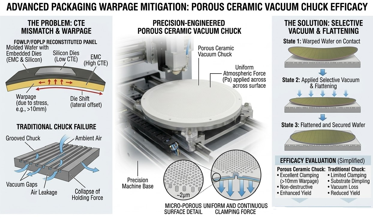
Why Porous Ceramic Vacuum Chucks Change the Load Distribution
A drilled or grooved chuck applies suction through discrete openings. A porous ceramic vacuum chuck passes air through a distributed network of small pores. When pore distribution, surface finishing, support structure, and flow resistance are properly engineered, the substrate experiences more continuous support and smaller unsupported spans.
That does not mean every porous chuck is automatically suitable. Performance depends on the complete assembly, including:
- Pore-size distribution rather than one nominal pore number.
- Surface flatness over the working diameter.
- Local and total airflow under full and partial coverage.
- Surface roughness and the risk of imprinting or particle trapping.
- Ceramic material, stiffness, chemical compatibility, and cleanliness.
- Base-plate design, bonding method, channels, seals, and vacuum control.
- Electrostatic behavior when charge-sensitive devices are handled.
The current Ceramic-Solutions wafer porous chuck range lists alumina and silicon carbide options, nominal pore choices from 0.5 to 20 µm, a listed porosity range of 30% to 70%, and flatness below 3 µm depending on total diameter. These are product-range values, not universal thresholds for OLED manufacturing. Final acceptance limits should be derived from the substrate, process pressure, panel size, and allowable topography.
Hole-Based and Porous Chuck Comparison
| Engineering factor | Discrete-hole or grooved chuck | Porous ceramic vacuum chuck | What to verify |
|---|---|---|---|
| Suction distribution | Concentrated at holes or channels | Distributed through a pore network | Pressure and flow map |
| Unsupported span | Set by hole diameter, groove width, and pitch | Related to pore structure and local support | Substrate topography under vacuum |
| Partial coverage | May create open leakage paths | Flow resistance can support partial adsorption | Holding force at minimum coverage |
| Surface imprint risk | Hole or groove pattern may transfer | Fine texture reduces pattern scale, but surface condition still matters | Witness-film and backside inspection |
| Cleaning behavior | Channels may be accessible | Pores require validated cleaning control | Flow recovery after cleaning |
| ESD behavior | Depends on chuck and grounding design | Depends on ceramic, coatings, and grounding path | Surface resistance and discharge plan |
How to Determine Whether the Vacuum Chuck Is the Root Cause
Match the Defect Signature
| Observed signature | More likely causes | Chuck-related evidence to seek |
|---|---|---|
| Repeating dots or grid | Hole pattern, print pattern, pixel/circuit pattern | Pitch and rotation match chuck openings |
| Long bands | Coating, drying, scanning, electrical rows | Bands change with chuck orientation or channels |
| Edge-to-center gradient | Thermal, coating, voltage drop, vacuum distribution | Pressure or flatness map shows the same trend |
| Random isolated spots | Particles, contamination, local film defects | Corresponding surface mark or particle |
| Gray-level-dependent non-uniformity | TFT or compensation behavior | Usually weak correlation with topography |
| Defect after bending or aging | Residual stress, encapsulation, electrical aging | Handling step created a repeatable stress concentration |
Run a Controlled Split Test
Use the same substrate lot and downstream recipe while changing one fixture variable at a time. Useful splits include:
- Standard chuck versus porous chuck.
- Two vacuum setpoints within the validated holding range.
- Original orientation versus a 90° chuck rotation.
- Full-area support versus controlled partial coverage.
- Before and after a documented cleaning cycle.
If the defect rotates with the chuck, follows vacuum pressure, or disappears when the unsupported span is reduced, the mechanical hypothesis becomes much stronger.
Connect Surface Metrology to Optical Data
The strongest evidence is a spatial correlation between physical and optical measurements. Depending on the process, the qualification plan may include:
- White-light interferometry or confocal topography of the held substrate.
- Backside inspection for dimples, particles, or imprinting.
- Pressure-sensitive or witness-film tests where compatible.
- Vacuum-flow and leak measurements at different coverage ratios.
- Panel luminance or chromaticity maps registered to chuck coordinates.
- Cross-correlation of defect pitch, orientation, and location.
A process team should define the coordinate transformation in advance. Without registration between the chuck, substrate, and optical image, a visual resemblance can be misleading.
Selecting a Porous Ceramic Vacuum Chuck for Flexible OLED Processing
A useful request for quotation should describe the process rather than asking only for a diameter and pore size. The broader semiconductor ceramics architecture—including the chuck body, base, seals, and mounting interface—should be reviewed as one system.
Substrate and Process Inputs
- Substrate material, thickness range, dimensions, and multilayer construction.
- Whether the substrate is free-standing, carrier-bonded, or framed.
- Process temperature, chemistry, cleanliness class, and allowable outgassing.
- Minimum and maximum coverage of the active chuck area.
- Required holding force and permitted pressure range.
- Allowable global flatness and local topography under vacuum.
- The optical, coating, printing, lamination, grinding, or metrology step performed while held.
Chuck Acceptance Criteria
- Flatness specified over the actual working area and temperature.
- Pore distribution and airflow uniformity, not only average pore diameter.
- Holding performance at both full and partial coverage.
- Surface-finish requirement tied to the substrate backside.
- Particle generation and cleaning recovery method.
- Edge exclusion, zoning, seals, and mounting interface.
- ESD or grounding requirements where relevant.
- A metrology report with agreed sampling density.
The best specification is an allowable substrate topography under real holding conditions. Chuck flatness by itself does not include deformation caused by pressure, seals, mounting, contamination, or the substrate's own mechanical properties.
When a Porous Chuck Will Not Solve the Mura
A fixture change cannot correct every OLED non-uniformity. It is unlikely to be the primary solution when the defect is dominated by TFT parameter spread, electrical supply distribution, mask or deposition non-uniformity, ink formulation, drying conditions, compensation data, or irreversible contamination introduced elsewhere.
Porous media also introduce their own engineering controls. Fine pores can clog; flow resistance can change after contamination; an unsuitable cleaning process can damage the working surface; and a very smooth but electrically insulating ceramic may require a separate ESD strategy. These limitations should be included in preventive maintenance and requalification plans.
The practical goal is not to label porous ceramic as a universal cure. It is to reduce one measurable mechanical risk—localized unsupported spans—while maintaining the vacuum stability, cleanliness, flatness, and electrical behavior required by the process.
Reducing OLED Mura requires a disciplined link between the visible defect and its manufacturing source. When optical maps correlate with vacuum geometry and substrate dimpling, a well-qualified porous ceramic vacuum chuck can remove a significant mechanical contributor. When that correlation is absent, the same framework redirects the investigation toward electrical, film-formation, thermal, or contamination causes instead of forcing the wrong fix.
Frequently Asked Questions
Need application-specific support for thin-substrate vacuum holding?
Contact Our TeamEngineering References
- Noh, Y. et al. “Controlling Drying Conditions in Vacuum for Uniform Film Formation in Inkjet-Printed OLEDs.” ACS Applied Materials & Interfaces (2024).
- Cordill, M. J. et al. “Measuring electro-mechanical properties of thin films on polymer substrates.” Microelectronic Engineering 137 (2015): 96-100.
- Kim, J. S. et al. “LTPO-based pixel circuit with highly uniform luminance and low flicker for variable refresh rate in AMOLED displays.” Scientific Reports (2025).
- Chen, H. et al. “Survey of Mura Defect Detection in Liquid Crystal Displays Based on Machine Vision.” Crystals 11, 1444 (2021).
- Crawford, G. P. “Flexible OLED displays using plastic substrates.” Proceedings of the IEEE (2003).