
Electrostatic Chucks
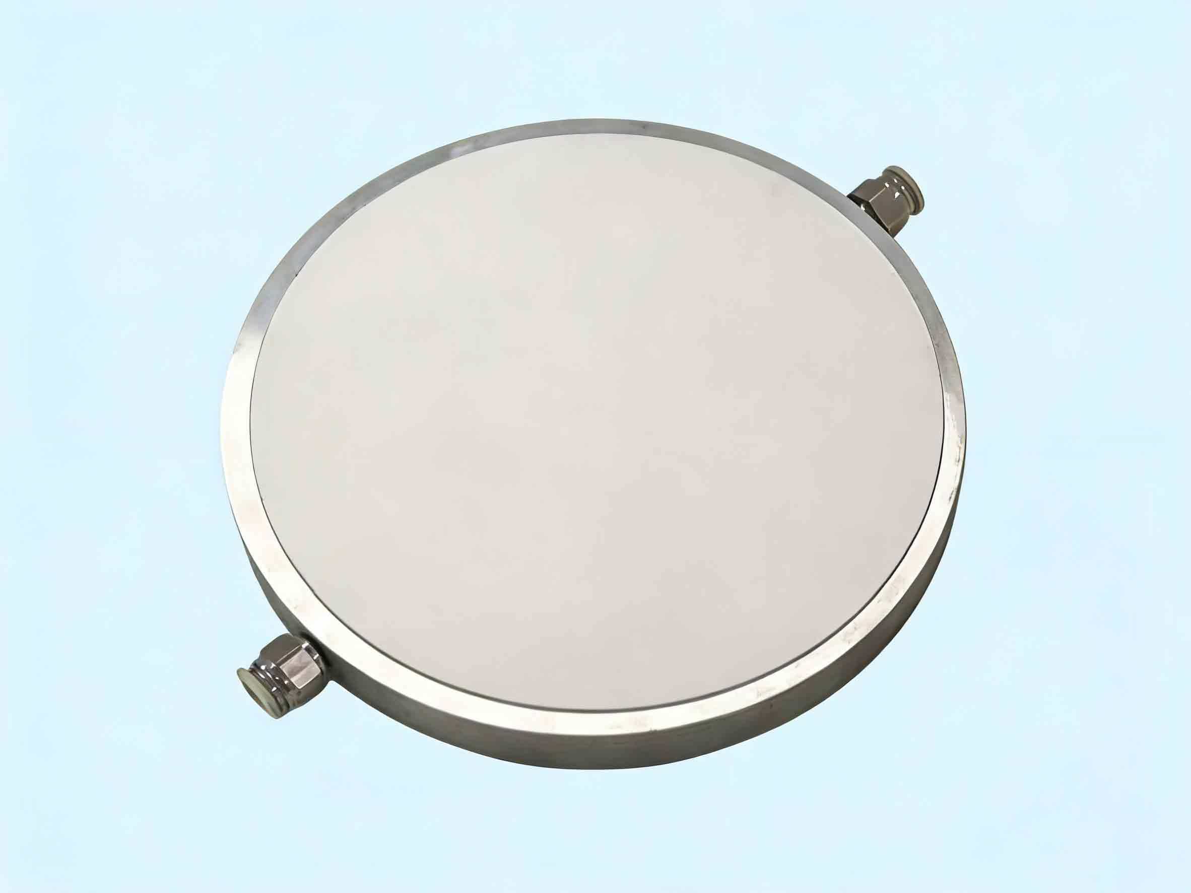
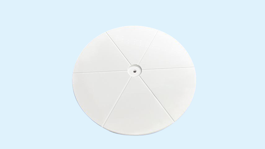
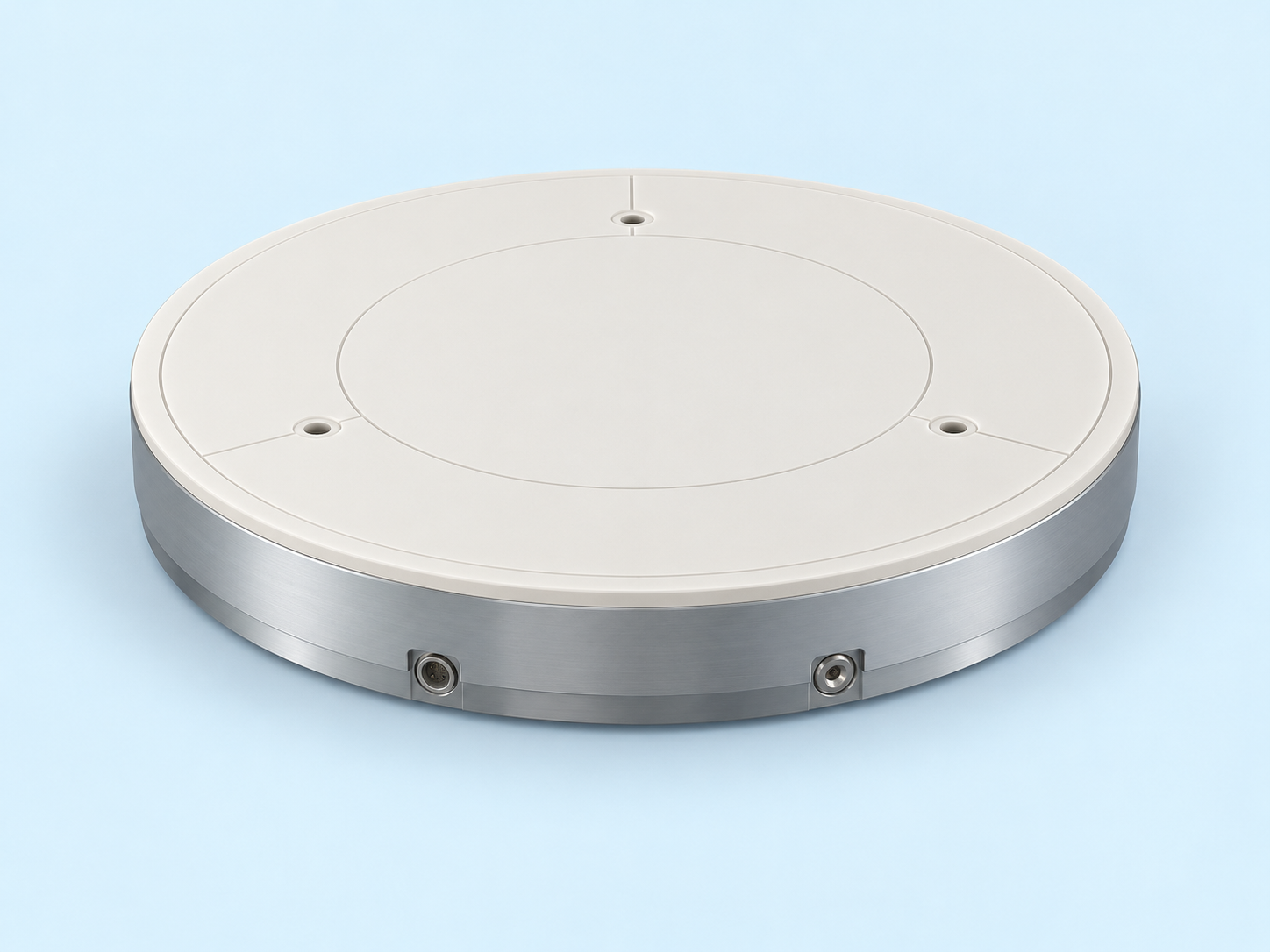
Cersol provides custom electrostatic chucks (ESCs) for semiconductor wafer holding and equipment integration. Each project is reviewed against the substrate, process environment, electrical system and mechanical interfaces. Material selection, electrode layout and operating limits require application-specific confirmation.
Electrostatic Wafer Holding
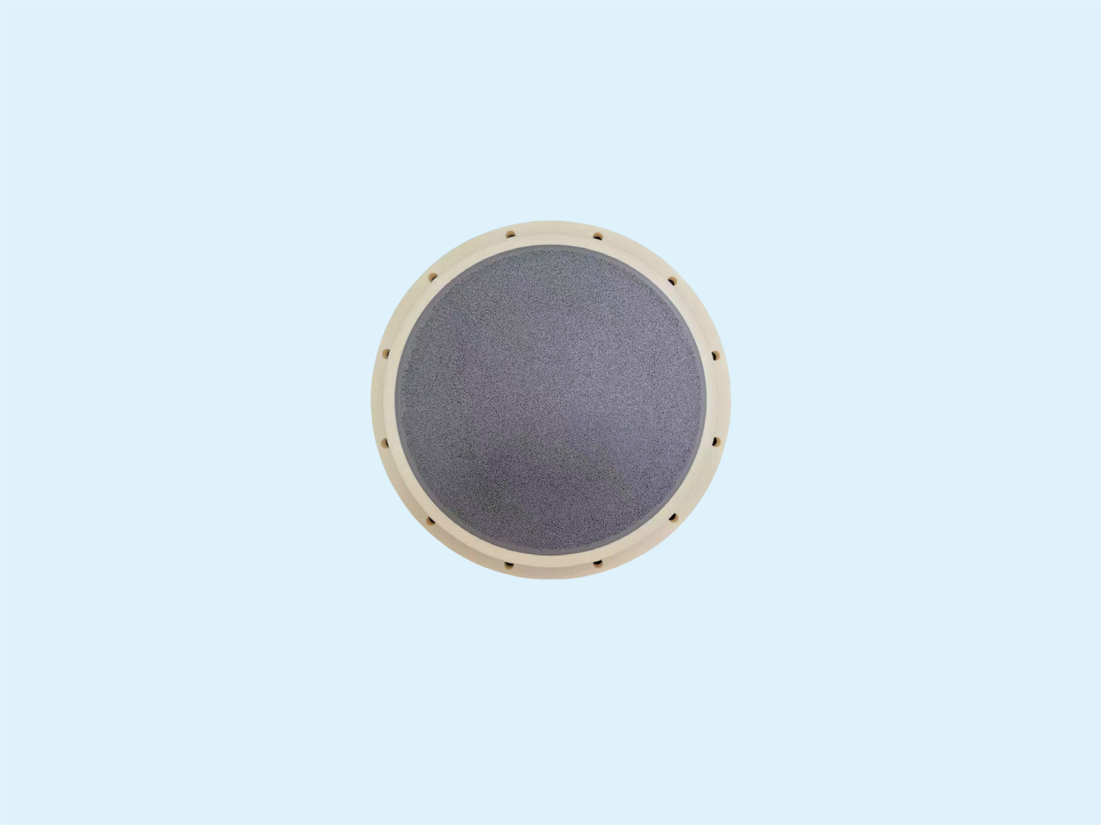
An electrostatic chuck uses an embedded electrode and a ceramic dielectric to create attraction between the chuck and the wafer. The wafer rests on the engineered chuck surface during operation. Holding force, wafer release and thermal behavior depend on the complete design and operating conditions.
Distributed Wafer Holding
Electrostatic attraction holds the wafer against the contact surface. Required holding performance must be assessed with wafer thickness, bow, backside condition and process loads.
Precision Surface Requirements
Flatness, surface finish and contact geometry are defined for the intended process and reviewed for manufacturing feasibility.
Reduced Edge Clamping
Compatible ESC designs can reduce reliance on mechanical edge clamps. The electrical design and release sequence remain part of equipment qualification.
Custom Equipment Interfaces
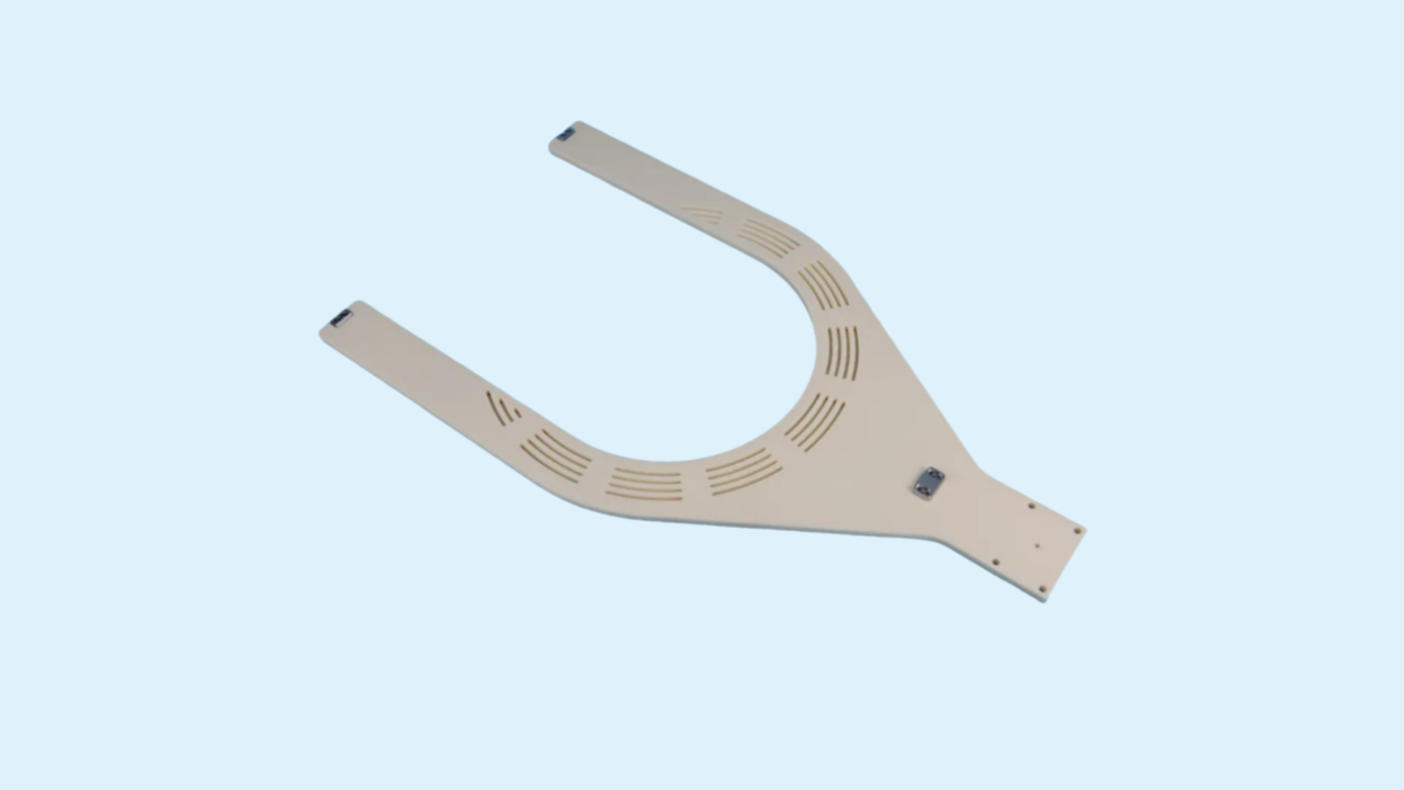
Chuck dimensions, mounting, electrode connections and other interfaces are evaluated against customer drawings and equipment requirements.
Technical Specifications and Design Inputs
| Product type | Electrostatic chuck (ESC) |
|---|---|
| Material system | Selected following review of electrical, thermal and process requirements |
| Electrode configuration | Monopolar or bipolar requirement to be reviewed for the project |
| Wafer or substrate | Specify material, diameter, thickness, backside film and allowable bow or warp |
| Operating voltage | Confirm with the ESC design, power supply and insulation requirements |
| Operating temperature | Confirm the process range, ramp rate, heat load and cooling conditions |
| Surface flatness and finish | Drawing-specific requirements, subject to manufacturing feasibility |
| Contact surface geometry | Specify lands, grooves, sealing areas and lift-pin interfaces where required |
| Process compatibility | Review vacuum conditions, process gases, plasma exposure and cleaning chemistry |
| Electrical and mechanical interfaces | Define connections, mounting, baseplate and equipment drawing requirements |
| Acceptance criteria | Agree holding and release performance, leakage limits, dimensional inspection and relevant process tests |
This table defines information needed for a custom project. It is not a standard model datasheet or a statement of guaranteed operating limits. Final specifications and acceptance criteria follow the agreed technical documentation.
Applications of Electrostatic Chucks
- Plasma etching: Wafer holding in compatible etching equipment, with assessment of plasma exposure, temperature and electrical conditions.
- Thin-film deposition: Wafer positioning in selected deposition processes where materials, surface design and operating limits meet process requirements.
- Precision semiconductor equipment: Custom wafer-holding projects requiring defined contact geometry, electrical connections and mechanical interfaces.
Application suitability is reviewed for the specific tool and process. A component suitable for one chamber or wafer condition should not be assumed interchangeable with another.
Design and Qualification
Electrical Design and Wafer Release
Review the available clamping power supply, wafer electrical properties, insulation requirements and allowable leakage current. Define the clamp and release sequence together with the equipment controls and wafer handling system.
Thermal and Process Compatibility
Specify the temperature range and process heat load. Where heating, cooling, backside gas or RF functions are required, include them in the initial technical brief so their feasibility can be evaluated with the chuck architecture.
Surface and Mechanical Integration
Provide the contact-area drawing, surface requirements, lift-pin locations, mounting details and electrical connection arrangement. Identify the inspection and functional tests required before equipment installation.
Information Needed for a Quotation
- Wafer material, size, thickness, backside condition and bow or warp.
- Equipment drawing, installation space, mounting and electrical interfaces.
- Process environment, temperature range, plasma conditions and cleaning chemistry.
- Required electrode arrangement, available voltage and current limits.
- Surface requirements, target holding and release behavior, and acceptance tests.
- Sample quantity, production requirements and requested delivery schedule.
For background on operating principles and material selection, see our ceramic electrostatic chuck technical guide.
Frequently Asked Questions
Is an electrostatic chuck a non-contact wafer holder?
No. The wafer rests on the engineered chuck surface. Electrostatic attraction provides holding force, while surface geometry and contact conditions influence performance.
Can an ESC replace a vacuum chuck directly?
A direct replacement should not be assumed. The holding principle, electrical supply, control sequence, interfaces and process conditions must be reviewed. See our porous ceramic chuck page for a separate wafer-holding option.
What voltage and temperature ratings are available?
These values require confirmation for the selected material system, electrode design and operating environment. Send your process requirements and equipment drawing for project-specific review.
Send your drawings and process requirements for a custom electrostatic chuck review.
Discuss Your ESC Project